| << Chapter < Page | Chapter >> Page > |
The converse of an interstitial impurity is when there are not enough atoms in a particular area of the lattice. These are called vacancies. Vacancies exist in any material above absolute zero and increase in concentration with temperature. In the case of compound semiconductors, vacancies can be either cation vacancies ( [link] c) or anion vacancies ( [link] d), depending on what type of atom are “missing”.
Substitution of various atoms into the normal lattice structure is common, and used to change the electronic properties of both compound and elemental semiconductors. Any impurity element that is incorporated during crystal growth can occupy a lattice site. Depending on the impurity, substitution defects can greatly distort the lattice and/or alter the electronic structure. In general, cations will try to occupy cation lattice sites ( [link] e), and anion will occupy the anion site ( [link] f). For example, a zinc impurity in GaAs will occupy a gallium site, if possible, while a sulfur, selenium and tellurium atoms would all try to substitute for an arsenic. Some impurities will occupy either site indiscriminately, e.g., Si and Sn occupy both Ga and As sites in GaAs.
Antisite defects are a particular form of substitution defect, and are unique to compound semiconductors. An antisite defect occurs when a cation is misplaced on an anion lattice site or vice versa ( [link] g and h). Dependant on the arrangement these are designated as either A B antisite defects or B A antisite defects. For example, if an arsenic atom is on a gallium lattice site the defect would be an As Ga defect. Antisite defects involve fitting into a lattice site atoms of a different size than the rest of the lattice, and therefore this often results in a localized distortion of the lattice. In addition, cations and anions will have a different number of electrons in their valence shells, so this substitution will alter the local electron concentration and the electronic properties of this area of the semiconductor.
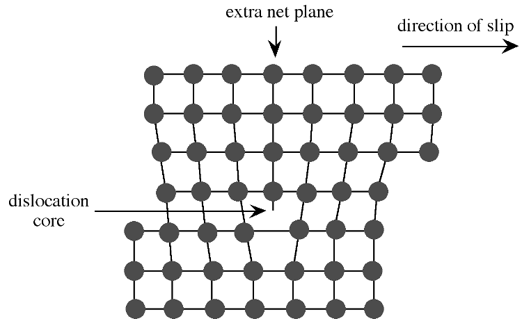
Extended defects may be created either during crystal growth or as a consequence of stress in the crystal lattice. The plastic deformation of crystalline solids does not occur such that all bonds along a plane are broken and reformed simultaneously. Instead, the deformation occurs through a dislocation in the crystal lattice. [link] shows a schematic representation of a dislocation in a crystal lattice. Two features of this type of dislocation are the presence of an extra crystal plane, and a large void at the dislocation core. Impurities tend to segregate to the dislocation core in order to relieve strain from their presence.

Epitaxy, is a transliteration of two Greek words epi , meaning "upon", and taxis , meaning "ordered". With respect to crystal growth it applies to the process of growing thin crystalline layers on a crystal substrate. In epitaxial growth, there is a precise crystal orientation of the film in relation to the substrate. The growth of epitaxial films can be done by a number of methods including molecular beam epitaxy, atomic layer epitaxy, and chemical vapor deposition, all of which will be described later.
Epitaxy of the same material, such as a gallium arsenide film on a gallium arsenide substrate, is called homoepitaxy, while epitaxy where the film and substrate material are different is called heteroepitaxy. Clearly, in homoepitaxy, the substrate and film will have the identical structure, however, in heteroepitaxy, it is important to employ where possible a substrate with the same structure and similar lattice parameters. For example, zinc selenide (zinc blende, a = 5.668 Å) is readily grown on gallium arsenide (zinc blende, a = 5.653 Å). Alternatively, epitaxial crystal growth can occur where there exists a simple relationship between the structures of the substrate and crystal layer, such as is observed between Al 2 O 3 (100) on Si (100). Whichever route is chosen a close match in the lattice parameters is required, otherwise, the strains induced by the lattice mismatch results in distortion of the film and formation of dislocations. If the mismatch is significant epitaxial growth is not energetically favorable, causing a textured film or polycrystalline untextured film to be grown. As a general rule of thumb, epitaxy can be achieved if the lattice parameters of the two materials are within about 5% of each other. For good quality epitaxy, this should be less than 1%. The larger the mismatch, the larger the strain in the film. As the film gets thicker and thicker, it will try to relieve the strain in the film, which could include the loss of epitaxy of the growth of dislocations. It is important to note that the<100>directions of a film must be parallel to the<100>direction of the substrate. In some cases, such as Fe on MgO, the [111] direction is parallel to the substrate [100]. The epitaxial relationship is specified by giving first the plane in the film that is parallel to the substrate [100].

Notification Switch
Would you like to follow the 'Chemistry of electronic materials' conversation and receive update notifications?