| << Chapter < Page | Chapter >> Page > |
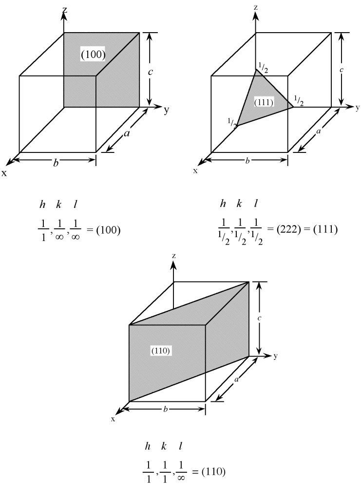
Planes in a crystal can be specified using a notation called Miller indices. The Miller index is indicated by the notation [ hkl ] where h , k , and l are reciprocals of the plane with the x , y , and z axes. To obtain the Miller indices of a given plane requires the following steps:
For example, the face of a lattice that does not intersect the y or z axis would be (100), while a plane along the body diagonal would be the (111) plane. An illustration of this along with the (111) and (110) planes is given in [link] .

As with crystal directions, Miller indices directions may be grouped in families. Individual Miller indices are given in parentheses ( hkl ), while braces { hkl } are placed around the indices of a family of planes. For example, (001), (100), and (010) are all in the {100} family of planes, for a cubic lattice.
Crystal structures may be described in a number of ways. The most common manner is to refer to the size and shape of the unit cell and the positions of the atoms (or ions) within the cell. However, this information is sometimes insufficient to allow for an understanding of the true structure in three dimensions. Consideration of several unit cells, the arrangement of the atoms with respect to each other, the number of other atoms they in contact with, and the distances to neighboring atoms, often will provide a better understanding. A number of methods are available to describe extended solid-state structures. The most applicable with regard to elemental and compound semiconductor, metals and the majority of insulators is the close packing approach.
Many crystal structures can be described using the concept of close packing. This concept requires that the atoms (ions) are arranged so as to have the maximum density. In order to understand close packing in three dimensions, the most efficient way for equal sized spheres to be packed in two dimensions must be considered.
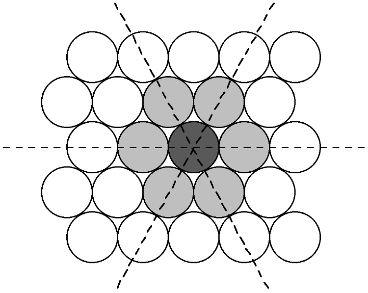
The most efficient way for equal sized spheres to be packed in two dimensions is shown in [link] , in which it can be seen that each sphere (the dark gray shaded sphere) is surrounded by, and is in contact with, six other spheres (the light gray spheres in [link] ). It should be noted that contact with six other spheres the maximum possible is the spheres are the same size, although lower density packing is possible. Close packed layers are formed by repetition to an infinite sheet. Within these close packed layers, three close packed rows are present, shown by the dashed lines in [link] .


Notification Switch
Would you like to follow the 'Chemistry of electronic materials' conversation and receive update notifications?