| << Chapter < Page | Chapter >> Page > |
SSPD_Chapter 7_Part 7_Scaling of MOS circuits.
7.7.1. What is scaling ?
Scaling is reduction in lateral and vertical dimensions to achieve a higher packing density on Si IC Chip, to achieve faster switching devices, to achieve higher functionality and achieve better scale of economy.
In 1966 emulsion mask patterns were contact printed using UV light on 200mm wafer with the smallest feature size of 25μm.
In 2007 using Deep Ultra Violet(DUV)193nm immersion Lithography, 30nm± 6 nm feature size are imprinted on 300mm wafer.
In 2012 using Extreme Ultra Violet Light(EUV)100nm reflective mirror exposure system (Next Generation Lithography-NGL), less than 30nm feature size is expected to be imprinted on 450mm wafer.
In 70s growth of Personal; Computer fueled the CMOS scaling.
Today in 21 st century, Internet, high speed communication that converges data, video and audio and mobile communication is fueling CMOS scaling consistent with Moore’s Law and has sharply brought in focus the need for cheap, high speed and low power devices for which Si:Ge is emerging as the the most promising candidate.
DSP and ‘DSP&Real World Interface’ are at the heart of Internet, so developing System-on-Chip(SOC) and integration of digital and Analog/RF function became high priority area of research. Advanced SiGe BJT Process also shrinks the lateral and vertical dimensions and boosts the performance hence it has become the technology of choice for 24GHz radar for blindside detection, for 77GHz radar system automobile collision warning or advance cruise control, for 60GHz Wi-Fi chips for next generation wireless LAN and backbone networks, for software defined radios, for cellular handset and for high frequency automatic test equipments.
7.7.2.How does scaling help achieve greater functionality ?
As we downscale the lateral and vertical dimensions we simultaneously add more functions to the chips.
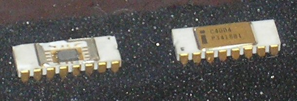
In 1971 μP4004 was a 16-pin DIP packaged chip which had the CPU built in the die. It was a LSI chip which along with three other LSI chips could be used to build a complete functional computer. These LSI chips were : 4001(ROM-4-bit output), 4002(RAM-4-bit input/output) and 4003 static shft register for expanding input/output lines. The photograph of the exposed 16-pin μP4004 chip and its hermetically shielded picture are shown in Figure 7.7.1.
4004 LSI chip used 10μm PMOS(E) technology. It had 2300 transistors and it could carry out 92,000 instructions per second that is 10.8μsecond per instruction.

Figure 7.7.1. Photograph of μP4004,16-Pin DIP packaged chip. Left is the exposed chip. Right is the hermetically sealed chip.

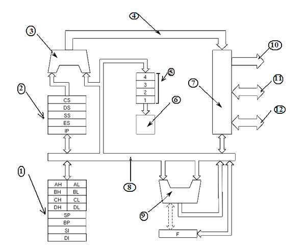
[1. Block of general purpose registers, 2 Block segment registers, 3 20 BIT combiner, 4 Internal bus C, 5 Queue commands, 6 The control system, 7 The control system bus, 8 Internal Bus A, 9 Arithmetic logic unit (ALU), 10 Address bus, 11 Data bus, 12 Rail Control F. Registry tags, AX -accumulator , BX - register base CX - counting register, DX - data register, SP - stack pointer, BP - base pointer, SI - source index, DI - Destination Index ,CS – code. Segment DS - data segment, SS - stack segment, ES - extra segment, IP - Instruction Pointer.]

Notification Switch
Would you like to follow the 'Solid state physics and devices-the harbinger of third wave of civilization' conversation and receive update notifications?