| << Chapter < Page | Chapter >> Page > |
SSPD_Chapter 7_Part 7_Scaling of MOS circuits_continued2
7.7.7. Scaling models and scaling factors.

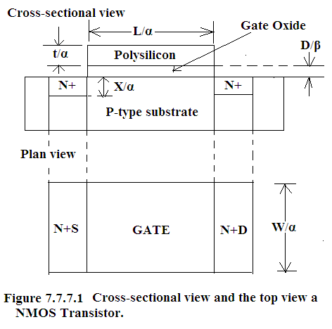
In Figure 7.7.7.1. NMOS cross-secctional view and top view are shown.
Linear dimensions both vertical and lateral are being scaled by 1/α..
DC Biasing voltage ,V DD , and Oxide thickness,D, are being scaled by 1/β.
We have three scaling models:
7.7.7.1.Scaling Factors for Device Geometrical parameters
1. Gate Area = A g = L×W. Each dimension is scaled by 1/α hence A g is scaled by 1/α 2 .
2.Gate Capacitance per unit area = C OX = ε 0 ε OX /D where D is scaled by 1/β therefore C OX is scaled by β.
3. Gate Capacitance , C g , = C OX ×LW has a scaling factor of β/α 2 .
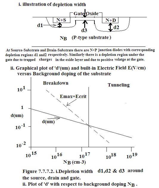
4. Parasitic Capacitance, C X = ε 0 ε Si A X /d= junction capacitance of the diode at Source-Substrate Junction and at Drain-Substrate Junction. ‘d’ is the depletion width of the diode. Since Source and Drain are at 0V and 5V respectively and substrate is also at 0V therefore depletion region around Source and Drain are d1 and d2 respectively extending primarily into P-Substrate because the two diodes are one-sided step junctions There is a depletion region d3 under the gate in the substrate. This is due to the trapped charges in the gate-oxide and due to the positive voltage a the gate electrode.

In Figure 7.7.7.1 cross-sectional view of NMOS structure with depletion region of ‘d’μm width is illustrated in the upper figure and in the figure below ‘d’μm’ plot with respect to Background doping of P-substrate is shown.
From Device Physics we know that for one-sided step junction:

As the channel length is scaled down, depletion region width ‘d’ must also be scaled down to prevent the source and drain depletion regions from meeting. This is probably to prevent “Punch Through” - a phenomena which occurs in BJT also.
During scaling, cross-sectuional area A X is scaled by 1/α 2 and Backgound Doping is increased so that d is scaled by 1/α.
So the scaling factor of C X is :

Increase in substrate doping N B decreases ‘d’ but increases threshold voltage V Th which is against the required trend of scaling and hence cannot be permitted therefore substrate doping is selectively increased around Source and Drain but not under the Gate by the application of deep channel implantation.
7.7.7.2.Scaling factors for different performance parameters for General Scaling Model.
i.Carrier density in the channel = Q ON = C OX ×V GS . (since V GS = V DD hence scaling factor for V GS is the same as for V DD ). Hence scaling factor for Q ON = β×(1/β) = 1
ii. Channel resistance R ON is given as follows:

Where ρ is resistivity of the ON channel and σ is the conductivity of the ON channel and

Where μ n = drift mobility of electrons since we are dealing with NMOS,
q= charge of an electron,
n n = number density or electron number per unit volume of the channel therefore

Substituting Eq.7.7.2.2 and Eq 7.7.2.3 in Eq.7.7.2.1 we get:

Therefore From Eq.7.7.2.4: R ON = (L/W)×[1/(μ n Q ON )]
Mobility is unaffected by scaling. Hence scaling factor is 1×1=1
iii Gate Delay τ d = C g R ON = (L×W)C OX ×(L/W)×[1/(μ n Q ON )] = L 2 C OX [1/(μ n Q ON )]
Therefore scaling factor of Gate Delay is (1/α 2 )×β×1= β/α 2 ;
iv Maximum toggle rate = f max = 1/τ d . Therefore the scaling factor is the reciprocal of that of Gate Delay i.e. (α 2 /β) .
v Saturation Current I DSS = (μ n C OX /2)(W/L)(V GS -V th ) 2 Here both V GS and V th are being scaled by (1/β). Hence the scaling factor is β×1×(1/β) 2 =1/β.
vi. Switching energy per gate E gate = (1/2)C g (V DD ) 2 . The scaling factor is (β/α 2 )(1/β) 2 =
1/(α 2 β).
vii. Power dissipation per gate P gate = Quiescent Power + Dynamic Power
= (V DD ) 2 /R ON + f max ×E gate . Hence the scaling factor is (1/β) 2 ×1+(α 2 /β)×(1/(α 2 β)
=1/β 2 .
viii. Power dissipation per unit area = P □ = P gate /A gate . Therefore the scaling factor = (1/β 2 )/(1/α 2 ) = (α/β) 2 .
ix. Power Speed Product is the Figure of Merit of the Gate = P gate × τ d . This has a scaling factor = 1/β 2 × β/α 2 =1/(βα 2 ).
Table 7.7.7.2.1. Scaling factors for different performance parameters for General Scaling Model.
| Performance parameter | Formula | Scaling Factor |
| Q ON | C OX ×V GS | 1 |
| R ON | (L/W)×[1/(μ n Q ON )] | 1 |
| τ d | C g R ON = L 2 C OX [1/(μ n Q ON )] | β/α 2 |
| Maximum toggle rate | f max = 1/τ d | (α 2 /β) |
| I DSS | (μ n C OX /2)(W/L)(V GS -V th ) 2 | 1/β |
| J DSS | I DSS /(L×W) | α 2 /β |
| E gate | (1/2)C g (V DD ) 2 | 1/(α 2 β) |
| P gate | (V DD ) 2 /R ON +f max ×E gate | 1/β 2 |
| P □ | P gate /A gate | (α/β) 2 |
| Figure of Merit | P gate × τ d | 1/(βα 2 ) |
7.7.7.3. Scaling factors for all the three scaling models.
In this section we will tabulate the scaling factors for all the three scaling models namely:
Table 7.7.7.3.1. Scaling Factors for long channel devices for the three scaling models.
| Parameter | Full Scaling | General Scaling | Fixed Scaling | |
| W,L,D | 1/α | 1/ α for W&L, 1/β for D | 1/ α | |
| V DD , V th | 1/ α | 1/β | 1 | |
| N B * | V/d 2 | α | α 2 /β | α 2 |
| Area/device | WL | 1/ α 2 | 1/ α 2 | 1/ α 2 |
| C OX = C □g | 1/D | α | β | 1 |
| C g | C OX WL | 1/α | β/ α 2 | 1/ α 2 |
| k n or k p | C OX W/L | α | β | 1 |
| I DSS | kV 2 | 1/ α | 1/β | 1 |
| t d | C g V/ I DSS | 1/ α | β/ α 2 | 1/ α 2 |
| P gate | C g V 2 /t d | 1/ α 2 | 1/β 2 | 1 |
| E gate | C g V 2 | 1 α 3 | 1/(β α 2 ) | 1/ α 2 |
*From Eq.7.7.7.1.1 :


Notification Switch
Would you like to follow the 'Solid state physics and devices-the harbinger of third wave of civilization' conversation and receive update notifications?