| << Chapter < Page | Chapter >> Page > |
SSPD_Chapter 7_Part 5_Stick Diagrams of Logic Gates_continued 2
7.5.1. NMOS inverter with (D)NMOS as pull-up transistor.
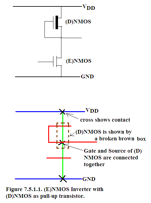
In Figure 7.5.1.1. we give the circuit diagram of (E)NMOS inverter with (D)NMOS as pull-up transistor.
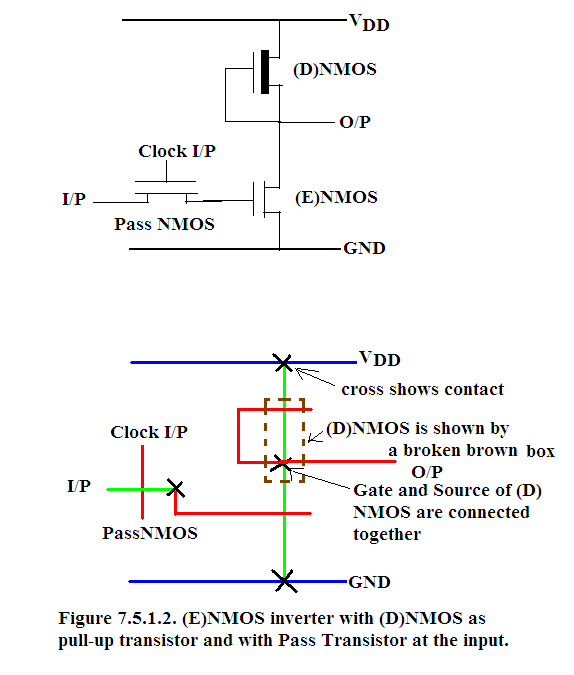
In Figure 7.5.1.2. we give the circuit diagram of (E)NMOS inverter with (D)NMOS as pull-up transistor along with a Pass Transistor at the INPUT.
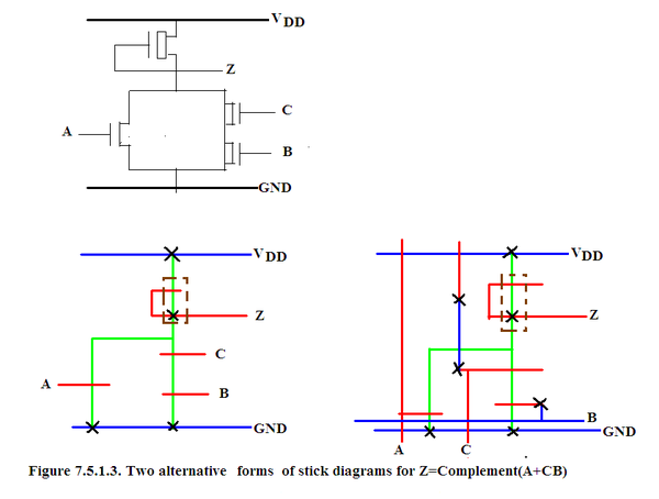
In Figure 7.5.1.3. we give the circuit diagram of Z= Complement of (CB+A) and its stick diagram.


In all these three diagrams, metal layer is the topmost layer, Poly-Si is intermediate layer and diffusion is the lowest layer. So crossing doesnot imply contact. Only when contact is made at the intersection of different layers that contact is made between different layers.
Also (E)NMOS is simply red line crossing green line but (D)NMOS is red line crossing green line within a broken brown box. This implies that N implant has been made under the Gate of (D)NMOS so that the transistor is normally-on.

Notification Switch
Would you like to follow the 'Solid state physics and devices-the harbinger of third wave of civilization' conversation and receive update notifications?