| << Chapter < Page | Chapter >> Page > |
SSPD_Chapter 7_Part 5_Stick Diagram of Logic Gates.
7.5 What is a Stick Diagram of a logic gate.
VLSI circuit is a 3-D set of patterned layers. Stick Diagram provides a top view of the patterns. Colours allow us to trace signal flow paths through conduction layers. It is a schematic of a circuit at physical design level.
Stick Diagram is a cartoon of the actual circuit. It is a circuit schematic with topology information but it has no real device size. It is not to scale and it uses color pencils to show the different layers of the device. Complicated wiring of gates and cells is easier to visualize with stick diagram. Planning and Physical Design using Stick Diagrams before going to CAD can save energy and time.
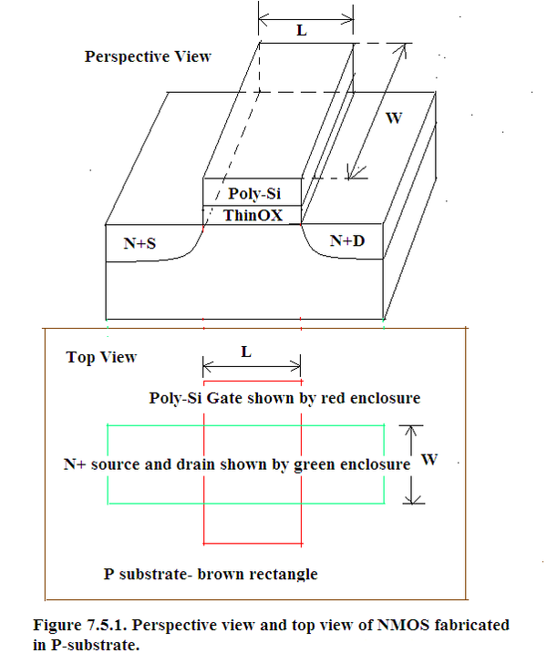
In Figure 7.5.1. the perspective view of (E)NMOS fabricated in P-Substrate is shown. At the bottom of the Figure 7.5.1. the top view of (E)NMOS fabricated in P-Substrate is given. The top-view contains the layout of the different layers of (E)NMOS:
Lowest layer is P-Substrate given by brown enclosure.
Second layer is N+ diffusion shown by green enclosure.
Topmost layer is Poly-Si shown by red colour.
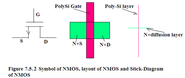
The symbol, the layout and the stick diagram of (E)NMOS is given in Figure 7.5.2.
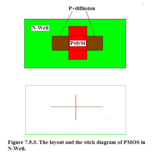
In Figure 7.5.3. the layout and the stick diagram of (E)PMOS in N-Well is shown.
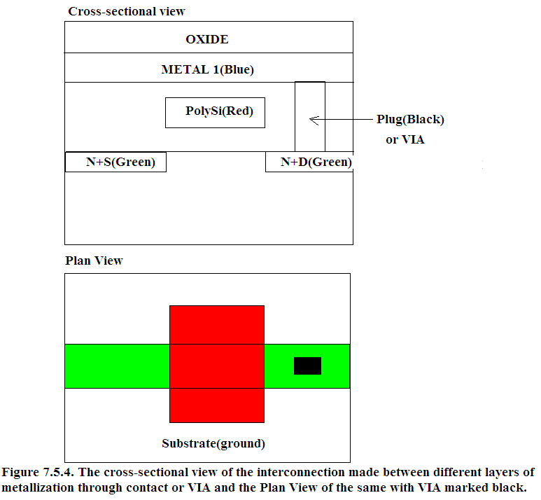
In Figure 7.5.4, the contact or VIA needed at two adjacent levels of metallization is shown.


Notification Switch
Would you like to follow the 'Solid state physics and devices-the harbinger of third wave of civilization' conversation and receive update notifications?