| << Chapter < Page | Chapter >> Page > |
2.1.3.2. Tri-Gate Devices now in production.
While the advantages of Tri-Gate transistors have been studied and known for some time, adoption and implementation is driven ultimately by technology and
manufacturability, as well as cost-effectiveness.
The advanced state of semiconductor manufacturing at very small geometries (40 nm, 28 nm, 22 nm or 20 nm and beyond) requires research and development expenditures
that now limit this technology to a handful of companies with capital expenditure capabilities in the billions of dollars. As a result, only a handful of manufacturers are
able to capitalize on the known advantages of 3-D transistor technology. Intel Corporation is the only company to have made this design and manufacturing
transition in 22 nm technology, and can provide data on the overall maturity and
manufacturability of Tri-Gate transistors on a mass production scale. This data, as of
the first quarter of 2013, includes 100 million units of Tri-Gate transistor-based
products.
Several known issues and characteristics of the 3-D gate structure have been
acknowledged and addressed to achieve manufacturing and design maturity with the
technology. These include the modeling of new parasitic capacitance values not
modeled in traditional planar designs, layout dependent effects, and the use of
double-patterning techniques using current lithographic equipment to form closely
spaced fins.
The electronic design automation (EDA) community is also an important factor in the maturity and usability of FinFET and Tri-Gate design technology to the
semiconductor designer. A great deal of publicity and user education is underway in
2013 by companies like Cadence and Synopsys revolving around the impact of
Tri-Gate rules and flexibility in the design of future semiconductor products.
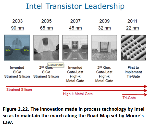
Intel has maintained its leadership in innovation in technology process so as to maintain the march along the Road Map laid down by Moore’s Law. Figure 2.22 shows the technology innovation introduced by INTEL in last decade of Semiconductor Manufacturing history.

In February 2013, Altera and Intel Corporation jointly announced that the next generation of Altera’s highest performance FPGA products would be produced using
Intel’s 14 nm 3-D Tri-Gate transistor technology exclusively. This makes Altera the exclusive major FPGA provider of the most advanced, highest performance semiconductor technology available.
2.1.3.3. Graphene Technology-the future generation IC enabler.
All this advancement and convergence in computation and communication was made possible due to scaling. But this is becoming more difficult as we go below 20nm process.[Hennessy, J; Patterson, De; “Computer Architecture”, 3 rd Edition, Morgan Kaufman Publishers, Amsterdam 2003].
According to International Technology Roadmap for Semiconductors (ITRS) we have the projection as given in Table 2.1.3.8
Table 2.1.3.8. Roadmap of CMOS Technology according to ITRS-2003
| Year | 05 | 06 | 07 | 08 | 09 | 10 | 11 | 12 | 13 | 14 | 15 | 16 |
|---|---|---|---|---|---|---|---|---|---|---|---|---|
| L Gate (nm) | 32 | 28 | 25 | 22 | 20 | 18 | 16 | 14 | 13 | 11 | 10 | 9 |
| ←Bulk/PartiallyDepleted-SOI→ | ||||||||||||
| ←Fully Depleted –SOI→ | ||||||||||||
| ←Multi-gate→ |

Notification Switch
Would you like to follow the 'Solid state physics and devices-the harbinger of third wave of civilization' conversation and receive update notifications?