| << Chapter < Page | Chapter >> Page > |
SRAM uses 6-Transistor to store a bit. SRAM is dominant form of embedded memory. It comprises 60- 70% chip area and 75% - 85% transistor count. As the logic gates density is increasing correspondingly the memory density must increase.
Statistical dopent fluctuations, variation in oxide thickness and line edge roughness increases the spread in V Th and I ON /I OFF in nano-scale regime [Murari 2003]. Increased leakage and parametric variations are making scaling of 6-T SRAM memory array difficult.
Due to fundamental physical limit to scaling, the era of conventional linear scaling of transistor dimensions has ended. Power dissipation and process induced variations have become the major issues for continued scaling of Si MOSFETs in future generation.
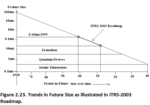
New materials and device structure are needed to continue the scaling trend as seen in ITRS-2003 Road map given in Figure 2.23.

According to ITRS 2003, by 2014 L Gate = 35nm, V DD = 0.4V and clock frequency = 30GHz.
Shrinking geometries, low power voltages and high frequency have a negative impact on
reliability. These enhanced features have increased the failure rates.
2.1.3.3.1. New and innovative methods to meet the challenges of nano miniaturization.
Multiple core with threading has been one innovation for solving the thermal management at nano level.
Copper interconnect provides higher electromagnetic threshold than Aluminum. So Industry is adopting Cu interconnects.
Fault avoidance and fault tolerance are the possible ways of improved reliability.
Fault avoidance relies on improved materials, improved manufacturing processes and improved circuit design. Cu interconnects is an example of improved materials.
SOI (Silicon-on-Insulator) is the process solution for lower circuit sensitivity to particle induced transients. Fault tolerance is implemented at circuit and system level. It relies on error detection and error correction code.
Human appetite for computation has grown faster than the processors power of real life computers. We need more powerful processors just to keep up with modern applications like interactive multi-media, mobile computing and wireless communication. In addition battery power is at premium in mobile computing environment hence power aware components/systems are indispensible.
Low power design can be achieved at different level of the system- basic process/device level (threshold reduction, multi-threshold deices), at circuit level (transistor sizing, logic optimization, activity driven power down, low swing logic, adiabatic switching), at architecture level (voltage scaling, parallelism,, instruction set , signal correlation) at algorithm level( complexity, concurrency, locality, regularity, data representation) and at system level.(design partitioning and power down).
We have to simultaneously look at performance-power-cost product . This will lead to new computer architecture.
As we scale down the dimensions for each new generation technology, new areas of applications are emerging.
To continue its historical growth and continue to follow Moore’s Law, the Semiconductor Industry will require advances at all fronts- from front end processors and lithography to design innovations, high performance process architecture and SOC solutions.
Further down the scaling strategy we are bound to hit a road block.
The recent development in the field of Graphene Transistors show that these could be a promising candidate for taking over the mantle for continued scaling down according to Moore’s Law.[Kreupl, Franz “ Carbon nano-tubes finally deliver”, Nature, . 484 , 321-322, 19 th April 2012; Franklin, Aaron D.;Luisier, Mathieu; Han, Shu-Jen;et.al. “Sub-10nm Carbon Nano tube Transistors”, Nano Letters Nature, 12, 758-762 (2012) ].
The present Graphene Transistor using single walled Carbon nano-tube(SWCNT) of 9nm at a supply voltage of 0.4V switches from ‘0’ to ‘1’. The current ratio of ON to OFF is 10,000 times which is excellent for LOGIC applications.. This operates at low voltage hence it mitigates the demand in energy. The only difficulty is in fabricating these devices because of non-availability of SWCNT of one flavor.
In contrast according to IRTS 2011[ITRS2011 Edition , Front End Processors, Go.nature.com/qykuh1(2011)], a similar sized Si MOSFET of 9nm gate length and operating at 0.64V will arrive in the market in 2022 and we cannot anticipate the cost.
So it is ripe time that we explore for alternatives if the present rate of miniaturization and development has to be maintained. The Future Generation Integrated Circuits is discussed in Chapter 8 of this Collectrion.

Notification Switch
Would you like to follow the 'Solid state physics and devices-the harbinger of third wave of civilization' conversation and receive update notifications?