| << Chapter < Page | Chapter >> Page > |
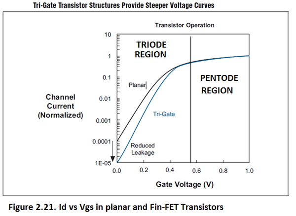
The power supply voltage can be significantly reduced with Tri-Gate without impairing its speed of operation due to increased effective width in Tri-Gate compared to planar transistor. The combination of lower supply voltage and reduced leakage current results in substantial power saving.

Fin-FET has a smaller cross-sectional area for the same performance of planar transistor.This gives a reduced area of incidence for cosmic particles which result into reduced Single-Event Error(SEE). This has been authenticated by 22nm implementation of Intel TriGate Fin-FET.
3-D Geometry and structure provides a host of improvements over planar structure as discussed above and enumerated below:
In 1974, IBM’s Robert Dennnard, inventor of single transistor DRAM(Dynamic RAM) showed that when MOSFET geometries, voltages and dopings were scaled down, gate transit time also scaled down and performance thus improved by the same factor. [“Design of Ion-Implanted MOSFET with very small Physical Dimensions”, IEEE Journal of Solid State Circuits, Vol.SC-9,No.5, 256-268,October 1974]. Taken together, density improvement as predicted by Moore’s Law and the performance improvement by Dennard signaled a coming explosion of growth in chip processing power. This precisely happened and this is what has been fueling Computer-Communication Revolution till date.
But there was great setback in 2005. Traditionally each new generation of Simanufacturing involves higher density and higher speed. But this scalng trend predicted above started plataeuing out at 90nm process technology. Clock rates stagnated as already pointed out above in Section 2.1.3. Power consumption and dissipation have grown with scaling. There was unacceptable gate leakage current. Therefore high-K(HfO, K=25) and metal gate technology was adopted. This maintained the improvement of performance by scaling till 40nm process technology.
On 4 th May 2011, Intel adopted Fin-FET (3D) Transistor for the manufacture of 22nm Semiconductor Products. Intel’s 22nm Tri-Gate uses 3 rd Generation high K/metal-gate scheme, copper interconnect, strained Si and 193nm Immersion Lithography.
International Technology Roadmaps for Semiconductor (ITRS) in 2012 identified 3-D Transistor Technology as the primary enabler of all incremental semiconductor improvements beyond 22nm process technology. 3-D Tri Gate is able to maintain the advantage below 22nm of higher packing density not by scaling but by extending the transistor width in the third dimension. This allows designers the ability to trade off the size and width of the transistor ‘fin’ based on performance, power, and transistor density packing objectives.
By adopting the 3-D technology, the steady march and consistent improvement in packaging density according to Moore’s Law has been maintained. This has meant steady improvement in performance, reduction in power back-up and reduction in cost per transistor. In addition there has been steady improvement in standby power and operating power dissipation.

Notification Switch
Would you like to follow the 'Solid state physics and devices-the harbinger of third wave of civilization' conversation and receive update notifications?