| << Chapter < Page | Chapter >> Page > |
Table.2.1.3.6.Comparative study of 2147/INTEL(1977) and 6147/Hitachi(1978).
| Product | HMOS 4kStaticRAM | Hi-CMOS4kSRAM |
|---|---|---|
| Technology | NMOS | Twin-well CMOS |
| Speed | 55/70ns | 55/70ns |
| I ACTIVE /I IDLE | 110mA/15mA | 15mA/1μA |
| Chip Size | 16.2nm 2 | 11.5nm 2 |
The Table clearly states that Hitachi CMOS memory is several orders of magnitude better than INTEL’s NMOS memory as far as standby power dissipation is considered. By 1981, CMOS 16k SRAM was manufactured and sold.
Table 2.1.3.7 gives the comparative study of microprocessor(μP) based on NMOS and CMOS.
Table 2.1.3.7.Comparative study of 6801/HIT(79) and 6301/HIT(81)
| Product | 6801/HIT(79)8-bit μP | 6301/HIT(81)8-bit μP |
|---|---|---|
| Technology | 4-μmNMOS | 3-μmCMOS |
| Speed | 1MHz | 1MHz,1.5MHz,2MHz |
| Power-Active | 900mW | 30mW(1MHz) |
| Stand-by Power | 70mW | 0.01mW |
| Pin Count | 40Pins | 40Pins |
EPSON introduced all CMOS computer HX-20 in 1982. It was a hand-held computer and proto-type/ancestor of the present day nomadic tools. Gradually all products are shifting to CMOS Technology.
Presently Digital Consumer Market(smart phones and Tablet PCs) is driving Semiconductor Industries. In coming day, Automotive market, Robotics, Medfical&Health Care and Sensor Network Market will be driving the Semiconductor Market.
The processor speed has increased 10 times from Pentium in 1993 to Pentium III in 1999 but with the introduction of Core2Duo in 2006 to Corei7 in 2013 the core speed has increased 1.5 times only but the appetite for high speed computing is insatiable. So obviously this paradigm of core computing will not be able to keep up with the computing needs of the post-industrial era. So new computing paradigms will have to be invented.
Breahthrough in Strained Silcon and High-K,metal gate Technology has allowed Fabless Companies to follow the Road Map set by Moore’s Law.
2.1.3.1. 3-D Tri-Gate Technology/Fin-FET Technology.
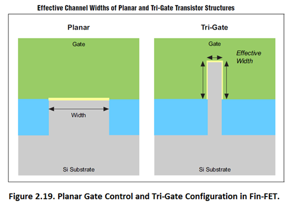
In 1991 a revolutionary 3D FinFET concept was put forward by Digh Hisamato and team of other researchers at Hitachi Central Research Laboratory. This proposed “WRAP AROUND” gate transistor technology. In conventional Planar Technology, GATE exercises control on the 2-D channel of electrons/holes only from the TOP.This new technology allowed the gate to exercise its control from 3 directions: From the TOP as well as from the TWO SIDES as shown in the Figure 2.19.

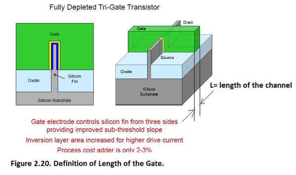
In Figure 2.19, the channel widths of Planar Transistor and Fin-FET are defined. In Figure 2.20 the channel length is defined in Fin-FET. The current drive capability and performance is directly proportional to its effective channel width as seen from the four Equations below:


The channel width can be significantly enhanced in 3-D Transistor structure in relation to planar structure because of the ability to extend the the width in the third dimension without increasing the layout area. This provides the potential for both enhanced design flecxibility for the designer as well as increased performance withput the same penality in 2-D area which exists when enhancing the width in planar transistor.
There is reduced active and leakage power in 3D Fin-FET transistors. This advantage results from the improved control of the channel by Gate’s electric field from the three sides of the Fin as shown in the figures. This results in a steeper curve of I D -V GS for Fin-FET as shown in Figure 2.21.The steeper curve results in significant reduction in leakage current in Fin-FET for the same performance of planar transistor or substantially higher performance in terms of operating speed or a combination of both.

Notification Switch
Would you like to follow the 'Solid state physics and devices-the harbinger of third wave of civilization' conversation and receive update notifications?