| << Chapter < Page | Chapter >> Page > |


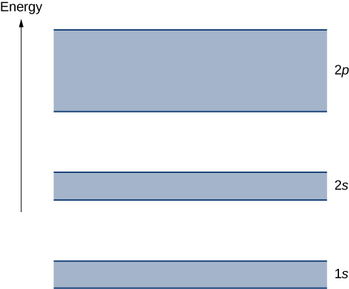
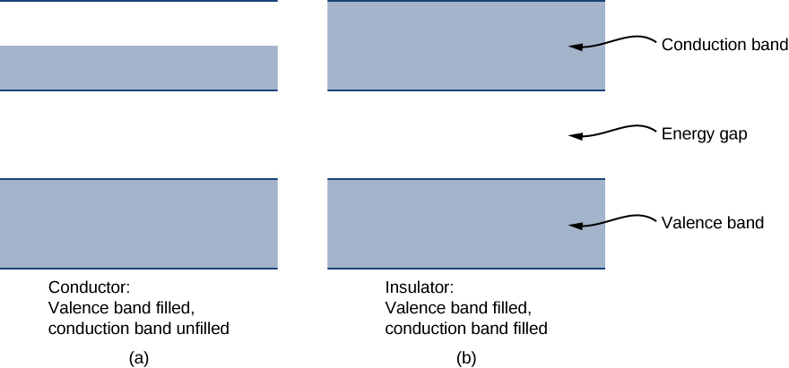
Each energy band is separated from the other by an energy gap . The electrical properties of conductors and insulators can be understood in terms of energy bands and gaps. The highest energy band that is filled is known as a valence band . The next available band in the energy structure is known as a conduction band . In a conductor, the highest energy band that contains electrons is partially filled, whereas in an insulator, the highest energy band containing electrons is completely filled. The difference between a conductor and insulator is illustrated in [link] .
A conductor differs from an insulator in how its electrons respond to an applied electric field. If a significant number of electrons are set into motion by the field, the material is a conductor. In terms of the band model, electrons in the partially filled conduction band gain kinetic energy from the electric field by filling higher energy states in the conduction band. By contrast, in an insulator, electrons belong to completely filled bands. When the field is applied, the electrons cannot make such transitions (acquire kinetic energy from the electric field) due to the exclusion principle. As a result, the material does not conduct electricity.

Visit this simulation to learn about the origin of energy bands in crystals of atoms and how the structure of bands determines how a material conducts electricity. Explore how band structure creates a lattice of many wells.
A semiconductor has a similar energy structure to an insulator except it has a relatively small energy gap between the lowest completely filled band and the next available unfilled band. This type of material forms the basis of modern electronics. At , the semiconductor and insulator both have completely filled bands. The only difference is in the size of the energy gap (or band gap ) E g between the highest energy band that is filled (the valence band) and the next-higher empty band (the conduction band). In a semiconductor, this gap is small enough that a substantial number of electrons from the valence band are thermally excited into the conduction band at room temperature. These electrons are then in a nearly empty band and can respond to an applied field. As a general rule of thumb, the band gap of a semiconductor is about 1 eV. (See [link] for silicon.) A band gap of greater than approximately 1 eV is considered an insulator. For comparison, the energy gap of diamond (an insulator) is several electron-volts.
| Material | Energy Gap |
|---|---|
What are the two main approaches used to determine the energy levels of electrons in a crystal?
(1) Solve Schrödinger’s equation for the allowed states and energies. (2) Determine energy levels for the case of a very large lattice spacing and then determine the energy levels as this spacing is reduced.
Describe two features of energy levels for an electron in a crystal.
How does the number of energy levels in a band correspond to the number, N , of atoms.
For N atoms spaced far apart, there are N different wave functions, all with the same energy (similar to the case of an electron in the double well of As the atoms are pushed together, the energies of these N different wave functions are split. By the exclusion principle, each electron must each have a unique set of quantum numbers, so the N atoms bringing N electrons together must have at least N states.
Why are some materials very good conductors and others very poor conductors?
Why are some materials semiconductors?
For a semiconductor, there is a relatively large energy gap between the lowest completely filled band and the next available unfilled band. Typically, a number of electrons traverse the gap and therefore the electrical conductivity is small. The properties of a semiconductor are sensitivity to temperature: As the temperature is increased, thermal excitations promote charge carriers from the valence band across the gap and into the conduction band.
Why does the resistance of a semiconductor decrease as the temperature increases?
For a one-dimensional crystal, write the lattice spacing ( a ) in terms of the electron wavelength.
What is the main difference between an insulator and a semiconductor?
For an insulator, the energy gap between the valence band and the conduction band is larger than for a semiconductor.
What is the longest wavelength for a photon that can excite a valence electron into the conduction band across an energy gap of 0.80 eV?
A valence electron in a crystal absorbs a photon of wavelength, . This is just enough energy to allow the electron to jump from the valence band to the conduction band. What is the size of the energy gap?
4.13 keV

Notification Switch
Would you like to follow the 'University physics volume 3' conversation and receive update notifications?