<< Chapter < Page Chapter >> Page >
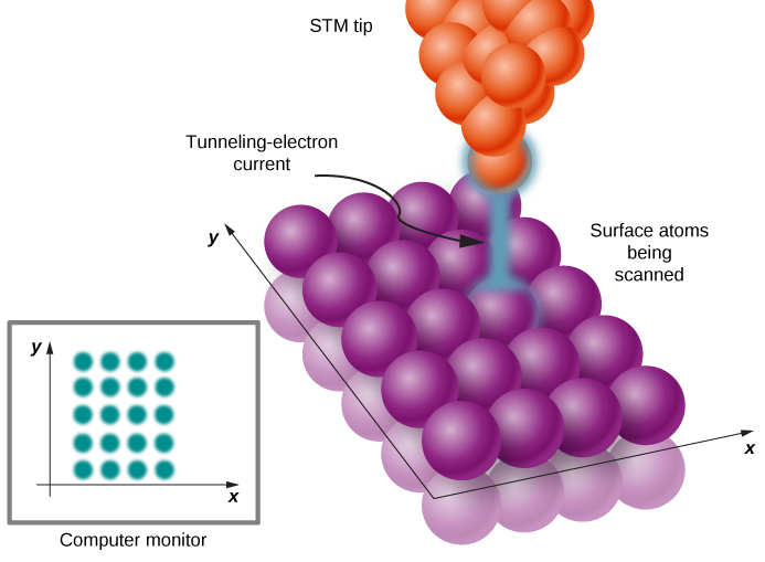
An illustration of a scanning tunneling microscope. The atoms in the tip and sample are represented by spheres, orange for the S T M tip and purple for the sample. The atoms on the surface of the atoms being scanned are arranged in this illustration in a grid of four atoms by five atoms. The tip is above one of the atoms, and a tunneling electron current is shown between the tip and the surface atom. The image on the computer monitor is a 4 by 5 grid of spots.
In STM, a surface at a constant potential is being scanned by a narrow tip moving along the surface. When the STM tip moves close to surface atoms, electrons can tunnel from the surface to the tip. This tunneling-electron current is continually monitored while the tip is in motion. The amount of current at location ( x , y ) gives information about the elevation of the tip above the surface at this location. In this way, a detailed topographical map of the surface is created and displayed on a computer monitor.
An STM image of a carbon nanotube showing the atoms as red points in a grid like pattern.
An STM image of a carbon nanotube: Atomic-scale resolution allows us to see individual atoms on the surface. STM images are in gray scale, and coloring is added to bring up details to the human eye.

Resonant quantum tunneling

Quantum tunneling has numerous applications in semiconductor devices such as electronic circuit components or integrated circuits that are designed at nanoscales; hence, the term ‘ nanotechnology    .’ For example, a diode (an electric-circuit element that causes an electron current in one direction to be different from the current in the opposite direction, when the polarity of the bias voltage is reversed) can be realized by a tunneling junction between two different types of semiconducting materials. In such a tunnel diode    , electrons tunnel through a single potential barrier at a contact between two different semiconductors. At the junction, tunneling-electron current changes nonlinearly with the applied potential difference across the junction and may rapidly decrease as the bias voltage is increased. This is unlike the Ohm’s law behavior that we are familiar with in household circuits. This kind of rapid behavior (caused by quantum tunneling) is desirable in high-speed electronic devices.

Another kind of electronic nano-device utilizes resonant tunneling    of electrons through potential barriers that occur in quantum dots. A quantum dot    is a small region of a semiconductor nanocrystal that is grown, for example, in a silicon or aluminum arsenide crystal. [link] (a) shows a quantum dot of gallium arsenide embedded in an aluminum arsenide wafer. The quantum-dot region acts as a potential well of a finite height (shown in [link] (b)) that has two finite-height potential barriers at dot boundaries. Similarly, as for a quantum particle in a box (that is, an infinite potential well), lower-lying energies of a quantum particle trapped in a finite-height potential well are quantized. The difference between the box and the well potentials is that a quantum particle in a box has an infinite number of quantized energies and is trapped in the box indefinitely, whereas a quantum particle trapped in a potential well has a finite number of quantized energy levels and can tunnel through potential barriers at well boundaries to the outside of the well. Thus, a quantum dot of gallium arsenide sitting in aluminum arsenide is a potential well where low-lying energies of an electron are quantized, indicated as E dot in part (b) in the figure. When the energy E electron of an electron in the outside region of the dot does not match its energy E dot that it would have in the dot, the electron does not tunnel through the region of the dot and there is no current through such a circuit element, even if it were kept at an electric voltage difference (bias). However, when this voltage bias is changed in such a way that one of the barriers is lowered, so that E dot and E electron become aligned, as seen in part (c) of the figure, an electron current flows through the dot. When the voltage bias is now increased, this alignment is lost and the current stops flowing. When the voltage bias is increased further, the electron tunneling becomes improbable until the bias voltage reaches a value for which the outside electron energy matches the next electron energy level in the dot. The word ‘resonance’ in the device name means that the tunneling-electron current occurs only when a selected energy level is matched by tuning an applied voltage bias, such as in the operation mechanism of the resonant-tunneling diode    just described. Resonant-tunneling diodes are used as super-fast nano-switches.

Questions & Answers

I'm interested in biological psychology and cognitive psychology
Tanya Reply
what does preconceived mean
sammie Reply
physiological Psychology
Nwosu Reply
How can I develope my cognitive domain
Amanyire Reply
why is communication effective
Dakolo Reply
Communication is effective because it allows individuals to share ideas, thoughts, and information with others.
effective communication can lead to improved outcomes in various settings, including personal relationships, business environments, and educational settings. By communicating effectively, individuals can negotiate effectively, solve problems collaboratively, and work towards common goals.
it starts up serve and return practice/assessments.it helps find voice talking therapy also assessments through relaxed conversation.
miss
Every time someone flushes a toilet in the apartment building, the person begins to jumb back automatically after hearing the flush, before the water temperature changes. Identify the types of learning, if it is classical conditioning identify the NS, UCS, CS and CR. If it is operant conditioning, identify the type of consequence positive reinforcement, negative reinforcement or punishment
Wekolamo Reply
please i need answer
Wekolamo
because it helps many people around the world to understand how to interact with other people and understand them well, for example at work (job).
Manix Reply
Agreed 👍 There are many parts of our brains and behaviors, we really need to get to know. Blessings for everyone and happy Sunday!
ARC
A child is a member of community not society elucidate ?
JESSY Reply
Isn't practices worldwide, be it psychology, be it science. isn't much just a false belief of control over something the mind cannot truly comprehend?
Simon Reply
compare and contrast skinner's perspective on personality development on freud
namakula Reply
Skinner skipped the whole unconscious phenomenon and rather emphasized on classical conditioning
war
explain how nature and nurture affect the development and later the productivity of an individual.
Amesalu Reply
nature is an hereditary factor while nurture is an environmental factor which constitute an individual personality. so if an individual's parent has a deviant behavior and was also brought up in an deviant environment, observation of the behavior and the inborn trait we make the individual deviant.
Samuel
I am taking this course because I am hoping that I could somehow learn more about my chosen field of interest and due to the fact that being a PsyD really ignites my passion as an individual the more I hope to learn about developing and literally explore the complexity of my critical thinking skills
Zyryn Reply
good👍
Jonathan
and having a good philosophy of the world is like a sandwich and a peanut butter 👍
Jonathan
generally amnesi how long yrs memory loss
Kelu Reply
interpersonal relationships
Abdulfatai Reply
What would be the best educational aid(s) for gifted kids/savants?
Heidi Reply
treat them normal, if they want help then give them. that will make everyone happy
Saurabh
Got questions? Join the online conversation and get instant answers!
Jobilize.com Reply

Get Jobilize Job Search Mobile App in your pocket Now!

Get it on Google Play Download on the App Store Now


Source:  OpenStax, University physics volume 3. OpenStax CNX. Nov 04, 2016 Download for free at http://cnx.org/content/col12067/1.4
Google Play and the Google Play logo are trademarks of Google Inc.

Notification Switch

Would you like to follow the 'University physics volume 3' conversation and receive update notifications?

Ask