| << Chapter < Page | Chapter >> Page > |
We have seen that the addition of specific elements to semiconductor materials turns them into p-type semiconductors or n-type semiconductors. The differences between n- and p-type semiconductors are summarised in [link] .
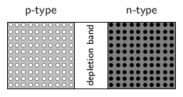
When p-type and n-type semiconductors are placed in contact with each other, a p-n junction is formed. Near the junction, electrons and holes combine to create a depletion region.

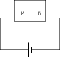
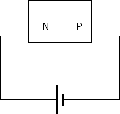
Electric current flows more easily across a p-n junction in one direction than in the other. If the positive pole of a battery is connected to the p-side of the junction, and the negative pole to the n-side, charge flows across the junction. If the battery is connected in the opposite direction, very little charge can flow.
This might not sound very useful at first but the p-n junction forms the basis for computer chips, solar cells, and other electronic devices.
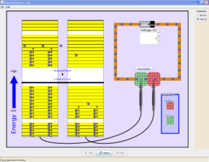
The following simulation allows you to see what happens in semi-conductors and to make semi-conductors.

In a p-n junction, without an external applied voltage (no bias), an equilibrium condition is reached in which a potential difference is formed across the junction.
P-type is where you have more "holes"; n-type is where you have more electrons in the material. Initially, when you put them together to form a junction, holes near the junction tends to "move" across to the n-region, while the electrons in the n-region drift across to the p-region to "fill" some holes. This current will quickly stop as the potential barrier is built up by the migrated charges. So in steady state no current flows.
Now when you put a potential different across the terminals you have two cases: forward biased and reverse biased.
Forward-bias occurs when the p-type semiconductor material is connected to the positive terminal of a battery and the n-type semiconductor material is connected to the negative terminal.

The electric field from the external potential different can easily overcome the small internal field (in the so-called depletion region, created by the initial drifting of charges): usually anything bigger than 0.6V would be enough. The external field then attracts more e- to flow from n-region to p-region and more holes from p-region to n-region and you have a forward biased situation. the diode is forward biased and so current will flow.

In this case the external field pushes e- back to the n-region while more holes into the p-region, as a result you get no current flow. Only the small number of thermally released minority carriers (holes in the n-type region and e- in the p-type region) will be able to cross the junction and form a very small current, but for all practical purposes, this can be ignored.
Of course if the reverse biased potential is large enough you get what is called avalanche break down and current flow in the opposite direction. In many cases, except for Zener diodes, you most likely will destroy the diode.
Semiconductors form the basis of modern electronics. Every electrical appliance usually has some semiconductor-based technology inside it. The fundamental uses of semiconductors are in microchips (also known as integrated circuits) and microprocessors.
Integrated circuits are miniaturised circuits. The use of integrated circuits makes it possible for electronic devices (like a cellular telephone or a hi-fi) to get smaller.
Microprocessors are a special type of integrated circuit.
Assess the impact on society of the invention of transistors, with particular reference to their use in microchips (integrated circuits) and microprocessors.

Notification Switch
Would you like to follow the 'Siyavula textbooks: grade 11 physical science' conversation and receive update notifications?