| << Chapter < Page | Chapter >> Page > |
We have seen that the size of the energy gap between the valence band and the conduction band determines whether a solid is a conductor or an insulator. However, we have seen that there is a material known as a semi-conductor. A semi-conductor is a solid whose band gap is smaller than that of an insulator and whose electrical properties can be modified by a process known as doping .
Doping is the deliberate addition of impurities to a pure semiconductor material to change its electrical properties.
Semiconductors are often the Group IV elements in the periodic table. The most common semiconductor elements are silicon (Si) and germanium (Ge). The most important property of Group IV elements is that they have 4 valence electrons.
Si has a band gap of J while Ge has a band gap of J.
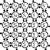
So, if we look at the arrangement of for example Si atoms in a crystal, they would look like that shown in [link] .

The main aim of doping is to make sure there are either too many (surplus) or too few electrons (deficiency). Depending on what situation you want to create you use different elements for the doping.
A surplus of electrons is created by adding an element that has more valence electrons than Si to the Si crystal. This is known as n-type doping and elements used for n-type doping usually come from Group V in the periodic table. Elements from Group V have 5 valence electrons, one more than the Group IV elements.
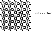
A common n-type dopant (substance used for doping) is arsenic (As). The combination of a semiconductor and an n-type dopant is known as an n-type semiconductor. A Si crystal doped with As is shown in [link] . When As is added to a Si crystal, 4 of the 5 valence electrons in As bond with the 4 Si valence electrons. The fifth As valence electron is free to move around.
It takes only a few As atoms to create enough free electrons to allow an electric current to flow through the silicon. Since n-type dopants `donate' their free atoms to the semiconductor, they are known as donor atoms .

A deficiency of electrons is created by adding an element that has less valence electrons than Si to the Si crystal. This is known as p-type doping and elements used for p-type doping usually come from Group III in the periodic table. Elements from Group III have 3 valence electrons, one less than the semiconductor elements that come from Group IV. A common p-type dopant is boron (B). The combination of a semiconductor and a p-type dopant is known as an p-type semiconductor. A Si crystal doped with B is shown in [link] . When B is mixed into the silicon crystal, there is a Si valence electron that is left unbonded.
The lack of an electron is known as a hole and has the effect of a positive charge. Holes can conduct current. A hole happily accepts an electron from a neighbor, moving the hole over a space. Since p-type dopants `accept' electrons, they are known as acceptor atoms .

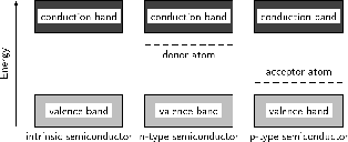
Donor (n-type) impurities have extra valence electrons with energies very close to the conduction band which can be easily thermally excited to the conduction band. Acceptor (p-type) impurities capture electrons from the valence band, allowing the easy formation of holes.

The energy level of the donor atom is close to the conduction band and it is relatively easy for electrons to enter the conduction band. The energy level of the acceptor atom is close to the valence band and it is relatively easy for electrons to leave the valence band and enter the vacancies.

Notification Switch
Would you like to follow the 'Siyavula textbooks: grade 11 physical science' conversation and receive update notifications?