| << Chapter < Page | Chapter >> Page > |
Thin films of many other materials have also been grown using MBE methods. Silicon technology has cheaper methods of growth and so Si layers are not very popular. However, possible devices made of Si-Ge alloys have been grown. The II-VI compounds, have also been grown. Magnetic materials, such as Co-Pt and Fe-Pt alloys, have been grown in the hopes of providing better magnetic storage.
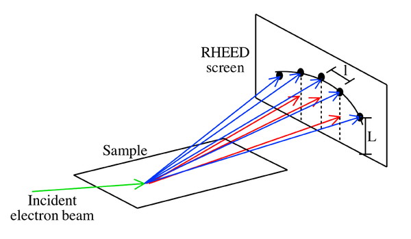
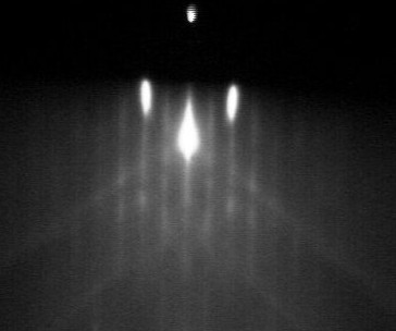
The most popular in-situ analysis technique for MBE-grown layers is reflection high energy diffraction (RHEED), see [link] . Electrons of energy 5 - 40 keV are directed towards the sample. They reflect from the surface at a very small angle (less than 3°) and are directed onto a screen. These electrons interact with only the top few atomic layers and thus provide information about the surface. [link] shows a typical pattern on the screen for electrons reflected from a smooth surface, in which constructive interference between some of the electrons reflected from the lattice structure results in lines. If the surface is rough, spots will appear on the screen, also. By looking at the total intensity of the reflected electron pattern, an idea of the number of monolayers deposited and how epilayers grow can be obtained. The island-type growth shown in this figure is an area of intense interest. These oscillations in intensity are gradually damped as more layers are grown, because the overall roughness of the surface increases.


Phase locked epitaxy takes advantage of the patterns of the oscillations to grow very abrupt layers. By sending the oscillation information to a computer, it can decide when to open or close the shutters of the effusion cell based on the location in the oscillation cycle. This technique self-adjusts for fluctuations in beam flux when the shutters are opened and can grow very abrupt layers.
Another analysis technique that can be used to study surface smoothness during growth is ellipsometry. Polarized laser light is reflected from the surface at a small angle. The polarization of the light changes, depending on the roughness of the surface.
Improved growth characteristics also require that the actual flux from the sources is measured. This is typically done with an ion gauge flux monitor, which is either used to measure residual beam that misses the substrate or is moved into the beam path for calibration when a new source is used. Because of the importance of clean substrate surfaces for low-defect growth, Auger spectroscopy is used following cleaning by sputtering. Auger spectroscopy takes place by ionizing an inner shell electron from an atom. When an outer shell electron then deexcites to the inner shell, the energy released can prompt the emission of another outer shell electron. The energy at which this occurs is characteristic of the atom involved and the signal can be used to detect impurities as small as 0.1%.

Notification Switch
Would you like to follow the 'Chemistry of electronic materials' conversation and receive update notifications?