| << Chapter < Page | Chapter >> Page > |
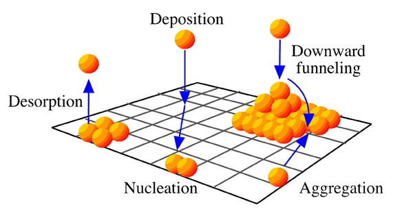
In the process of epitaxy, a thin layer of material is grown on a substrate. With respect to crystal growth it applies to the process of growing thin crystalline layers on a crystal substrate. In epitaxial growth, there is a precise crystal orientation of the film in relation to the substrate. For electronic devices, the substrate is a single crystal (usually Si or GaAs) and therefore so is the epitaxial layer (epilayer). In the most basic form of molecular beam epitaxy (MBE), the substrate is placed in ultra high vacuum (UHV) and the source materials for the film are evaporated from elemental sources. The evaporated molecules or atoms flow as a beam, striking the substrate, where they are adsorbed on the surface. Once on the surface, the atoms move by surface diffusion until they reach a thermodynamically favorable location to bond to the substrate. Molecules will dissociate to atomic form during diffusion or at a favorable site. [link] illustrates the processes that can occur on the surface. Because the atoms require time for surface diffusion, the quality of the film will be better with slower growth. Typically growth rates of about 1 monolayer per second provide sufficiently high quality.

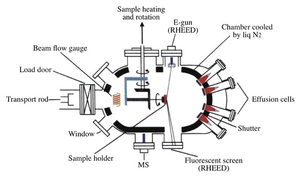
A typical MBE chamber is shown in [link] . The substrate is chemically washed and then put into a loading chamber where it is further cleaned using argon ion bombardment followed by annealing. This removes the top layers of the substrate, which is usually an undesired oxide which grew in air and contains impurities. The annealing heals any damage caused by the bombardment. The substrate then enters the growth chamber via the sample exchange load lock. It is secured on a molybdenum holder either mechanically or with melted indium or gallium which hold the substrate by surface tension.

Each effusion cell (see [link] ) is a source of one element in the film. The effusion cell, also called a Knudsen cell, contains the elemental form in very high purity (greater than 99.99999% for Ga and As). The cell is heated to encourage evaporation. For GaAs growth, the temperature is typically controlled for a vapor pressure of 10 -2 to 10 -3 Torr inside the effusion cell, which results in a transport of about 10 15 molecules/cm 2 to the substrate when the shutter for that cell is opened. The shape and size of the opening in the cell is optimized for an even distribution of particles on the substrate. Due to the relatively low concentration of molecules, they typically do not interact with other molecules in the beam during the 5 - 30 cm journey to the substrate. The substrate is usually rotated, at a few rpm, to further even the distribution.

Notification Switch
Would you like to follow the 'Chemistry of electronic materials' conversation and receive update notifications?