| << Chapter < Page | Chapter >> Page > |

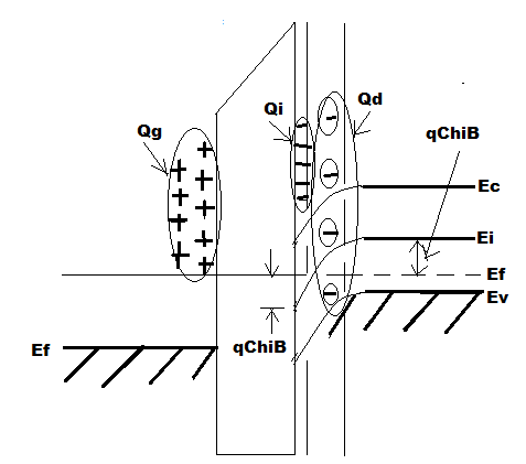
Figure 6.36. Ideal MOS diode with gate bias exceeding threshold voltage.
The n type channel has its electrons thermally generated hence its response is slow. Therefore when small signal capacitance is measured at HF then the rapid variation in gate charge can be matched only by the rapid variation in depletion width d max. and hence ΔQ g is balanced ΔQ d .
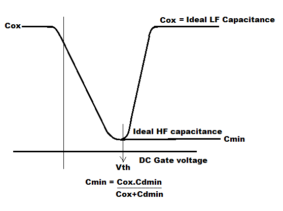
Therefore the capacitance measured is:
C min = series combination of C ox and C Dmin =[ (C ox × C Dmin ) / (C ox + C Dmin )]_______(6.9)
Where C Dmin = = [ε 0 ε Si A/d max ]_________________________________________(6.10)
But under the same DC gate voltage if LF(Low Frequency) small signal capacitance is measured then ΔQ g is balanced by ΔQ i instead of ΔQ d because under low speed variation condition or under steady state condition electrons of the inversion layer can easily be thermally generated or recombined. Hence LF capacitance measured will be C ox as shown in Figure 6.37

Figure 6.37 Ideal MOS capacitance curves at high and low frequencies.
But in reality , depending on the preparation conditions of the oxide, how it was formed and so on, will determine what electrical characteristics you have.In actual practice the position of the shape of C-V measurement in Figure 3.37 is not obtained.
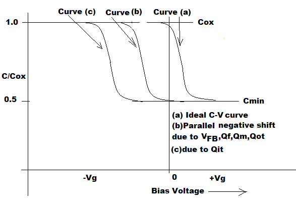
The position of that capacitance drop along the voltage axis compared to a corresponding theoretical plot, is a measure of the number of charges in the oxide.
The more positive charges in the oxide, for instance, the point where the capacitance drops along the voltage axis will move to the left, to more negative values as shown in Figure 6.38. If you have, for instance, negative charges in the oxide, the curve will be shifted in the positive direction compared to the theoretical plot.

Figure 6.38 Departure or parallel shift from Ideal Curve (a) due to flat band voltage V FB , Fixed Oxide Charge (Q f ), Mobile Oxide Charge (Q m ), Interface trapped Charge ( Q it ), Oxide trapped Charges ( Q ot )
We can measure the position of the C-V curve along the voltage axis before and after moving the sodium ions from the field plate interface to the silicon oxide interface using a bias-temperature stress test. You can move them back and forth and watch the C-V curve shift back and forth. This gives you a tool to measure the effect of all sorts of process conditions on charge formations. Stress conditions are normally ±50V/um of oxide, 300° C, and 2 minutes.
Table 6.9 Comparative study of density of various charges in two different orientations Si crystals
| <100> | <111> | |
| Qit | 10 10 /cm 2 /eV | 10 11 /cm 2 /eV |
| Qf | 10 10 /cm 2 | 5×10 10 /cm 2 |
All four types of charges have deleterious effect on device operation. During fabrication we choose process sequences which will minimize the charges. By high temperature inert anneals in Ar and N 2 towards the end of the process flow and a moderate 400°C anneal in H 2 or forming gas (N 2 /H 2 ) at the end of the process accomplishes this.
The instabilities that had been noted over these years in thermal oxides and MOS transistors, were actually due to mobile ions, like sodium, lithium, potassium. Very interesting series of events were occurring, in that there were several laboratories working on the same problem. IBM, RCA, Bell Laboratories, Philco and a couple of others.
In '64 the PLANAR-II technology was introduced for the fabrication of stable MOS. The PLANAR-II was a term that was used to denote stable MOS.
In order to fabricate stable MOS we go through the following steps:
1.Using a clean metallization system, that is using electron-beam metallization, rather than filament metallization, which had been used previously.
2.To minimize the sodium incorporation into the process gettering steps were used. Here phosphorous is deposited on Silicon Dioxide to form phosphosilcate glass (PSG). This PSG is used to actually suck the impurity ions out of the oxide after they get in there. Impurity got in there after all of the attempts to keep them out.
To stabilize MOS device a vapor-deposited oxide is needed at the final stage of fabrication. This is needed for passivation and stable performance where the oxide is produced in the vapor phase and deposited over the device or circuit. We cannot do thermal oxidation as it is done after metallization. The process that was initially used was called TEOS, which was tetraethylorthosilicate.
A process which involved the breakdown of a organic oxygen-containing compound to form SiO2. This was done at about 750 degrees. The problem with this process is 750 degrees is way over the melting point of aluminum, and we desired to have something that would go down under 450 degrees, be deposited at less than 450 degrees. Silane, SiH4, can be reacted with oxygen, to produce SiO2. Again, a vapor-deposited process, but it would be deposited around 400 degrees. This helped achieve deposited oxide that would go over an integrated circuit, having metallized aluminum as the interconnect material.. Now it's quite a standard process. This standard process has added plasma, activated process with plasma, which produces a more even, uniform oxide.
Once the fabrication of stable MOS was achieved it became the brick for building all of the microprocessors.

Notification Switch
Would you like to follow the 'Solid state physics and devices-the harbinger of third wave of civilization' conversation and receive update notifications?