| << Chapter < Page | Chapter >> Page > |
2.1.2.1.Main Frame Era.
In 1956, Sperry Rand,USA, commercialized 2 nd Generation Main Frame Computers by the brand name of UNIVAC II. This was a hybrid of Vacuum Tube (5,200 Tubes) and BJT (1,200 Transistors) hence size and power consumption was reduced but it did not carry the distinct hall mark of Solid State Era. But it was a great improvement over ENIAC in terms of weight, physical size and power consumption. Also it was Storage Program Computer whereas through Plugboard Control ENIAC had to be manually adjusted for running different programs.
On 13 th September 1956, IBM 305 RAMAC Computer with disk-drive was commercialzed. It was still a Vacuum –Tube version but it had secondary storage space of 4.4MegaBytes on 350 disk file. This 350 disk file had 24ʹʹ magnetically coated platters 50 in number. Today we can store 70GB information in Hard Disc of computers.
1959 was the turning point in Solid State Era. Robert Noyce of Fair-Child and Jack Kilby of Texas Instruments simultaneously invented the magic chip called Integrated Circuits Micro-Chip. This became the enabling technology of our present on-going Computer-Communication Revolution. This became the engine of growth of Semiconductor Industry. This IC Chip made electronics, electronics communication and electronics computation accessible to one and all. IC Chips made application of Electronics Systems adaptable and suitable for all domains of life. IC Chips are being used by Military, Trade&Commerce, Entertainment, Transportation, Health-care , Industrial Manufacturing , Agricultural production and mining. The list goes on. Every day brings a new domain under the perview of Electronics IC Chip.

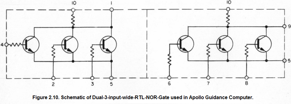
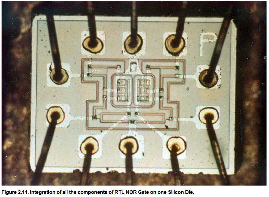
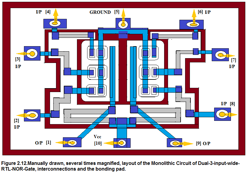
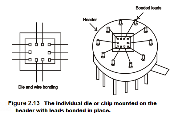
In Figure 2.10, the schematic of Dual-3-input-wide-RTL-NOR-Gate is shown. This has been integrated on a Si-die, mounted on a header, gold-wire bonded to the 10 leads of the header by Thermo-compression Bonding and hermetically sealed. The Si-die on which the circuit has been integrated is shown in Figure 2.11. In Figure 2.11, the top-view of the Planar Circuit is shown. It shows the transistors, its interconnections and bonding pad layout. The golden wires bonded to the bonding pads of the circuit and to the external leads of the header are also shown. The external leads of the header are not visible. In Figure 2.12, manually drawn layout of the circuit is shown. It is identical to the layout in Figure 2.11. Thermo-compression bonding of the gold wire to the bonding pads on the Si-Die and to the external leads of the header are shown in Figure 2.13 and hermetic shielding and packaging are shown in Figure 2.14. We have two kinds of packaging: Dual-in-Line Package (DIP) and TO-5 Package. For low power dissipation Ceramic DIP is used whereas for large power dissipations, metal can TO-5 package is more suitable and it can be mounted on a heat sink to prevent thermal run-away condition.


5 th October 1959, the legendary IBM 1401 Data Processing System was introduced. A very good description of this main frame computer is given in the article :

Notification Switch
Would you like to follow the 'Solid state physics and devices-the harbinger of third wave of civilization' conversation and receive update notifications?