<< Chapter < Page Chapter >> Page >
This module gives a brief overview of the MSP430™ microcontroller, how to read a data sheet for an MSP430™ microcontroller, and how to pick the right one for some sample applications. This module is one of many in a textbook designed to help seniors select TI products for use in their senior project.

MSP430™ microcontrollers

MSP430™ microcontrollers (MCUs) from Texas Instruments are 16-bit, RISC-based, mixed-signal processors designed specifically for ultra-low power. MSP430 MCUs have the right mix of analog and digital integrated intelligent peripherals, ease of use, low cost and lowest power consumption for thousands of applications ranging from simple sensor designs to complex electricity meters.

To get a better idea of what the MSP430 MCU is and how you can use it to solve a system design need or application problem, let’s take a look at a typical block diagram for a device. Figure 1 is the device block diagram for the MSP430G2553, one of the MSP430 Value Line devices.
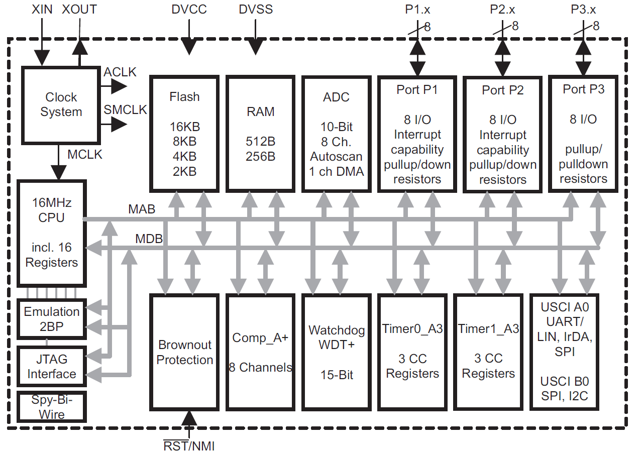
The purpose of the block diagram is to provide a high-level reference of the integration and feature set found in a given device. You can find the block diagram for any MSP430 MCU in the data sheets at www.msp430.com .

The block diagram contains key features of the device that can help you quickly identify if an MSP430 MCU is a fit for a given application need. There are a few features you will need to consider:

  • Integrated memory:
    • Includes both volatile (RAM) and nonvolatile (flash) sizes.
    • When multiple values are listed, it shows which device memory size variants are available with the same peripherals.
  • General-purpose I/O pins:
    • The MSP430G2553 has up to 24 I/Os available: eight Port1 (P1), eight P2 and eight P3 I/Os.
      • Package-dependent: Check the pinout for the total number.
    • All pins have configurable integrated pullup or pulldown resistors.
    • P1 and P2 I/Os when inputs can provide an interrupt to the CPU.
  • CPU and emulation capabilities:
    • 16 MHz is the maximum CPU clock speed for the MSP430G2553.
    • Integrated emulation for the MSP430G2553 has two hardware breakpoints (2BP) for use when debugging.
  • Simplified clock system:
    • One external clock source on XIN/XOUT can be sourced.
    • The internal clock tree provides three clock tree branches.
  • Digital and analog peripheral mix. The MSP430G2553 device includes:
    • 10-bit, eight-channel analog-to-digital converter (ADC) with internal voltage reference for voltage measurement (sensors, power rails, etc).
    • Comp_A+: eight-channel analog comparator with internal voltage reference for simple measurements or voltage threshold detection.
    • WDT+: watchdog timer for resetting the CPU in case of timeout (can also be used as a simple interval timer generating an interrupt).
    • Timer0,1_A3: two 16-bit general-purpose timers, each with three capture-compare (CC) I/Os.
    • USCI (A0/B0): universal serial communication interface module capable of providing standard UART, SPI and I2C communication protocols used to interface with external digital devices (sensors, data converters, radio ICs).

Figure 2 is the corresponding pinout also found in each device data sheet for the MSP430G2553. Here you can see exactly how peripheral functions are mapped onto the multiplexed I/Os of the device. Each I/O pin can be configured in software to provide the desired pin function for a given I/O based on its internal connectivity.

Get Jobilize Job Search Mobile App in your pocket Now!

Get it on Google Play Download on the App Store Now


Source:  OpenStax, Senior project guide to texas instruments components. OpenStax CNX. Feb 12, 2013 Download for free at http://cnx.org/content/col11449/1.3
Google Play and the Google Play logo are trademarks of Google Inc.

Notification Switch

Would you like to follow the 'Senior project guide to texas instruments components' conversation and receive update notifications?

Ask