| << Chapter < Page | Chapter >> Page > |
Crystal Growth-Bulk and Epitaxial Film_Part 4
EPITAXIAL FILM GROWTH.
There are two major epitaxial film growth technologies:
Silicon Epitaxial Film Growth Technology (Low End Technology hence economical) and Compound Semiconductor Epitaxial Film Growth Technology (High End Technology hence expensive and suitable for niche applications).
Silicon Epitaxial Film Growth Technology are further divided into:
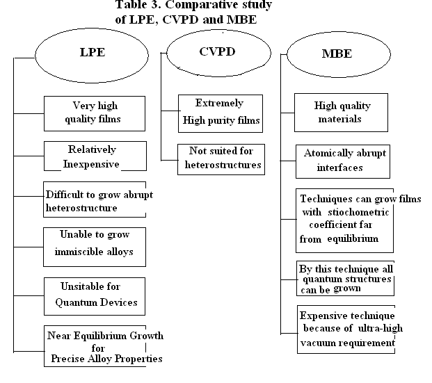
Chemical Vapour Phase Deposition(CVPD) Technology and Liquid Phase Epitaxy(LPE). LPE is relatively cheaper but very toxic.
Compound Semiconductor Epitaxial Film Growth is achieved by Molecular Beam Epitaxy System which is inordinately expensive and in India in a few places only we have MBE systems namely TIFR(Mumbai), Solid State Physics Laboratory(Delhi), Central Electronics Engineering Research Institute (Pilani), IIT(Madras) and CSIO(Chandigarh).
In Table 3 we make a comparative study of LPE, CVPD and MBE. Molecular Beam Epitaxy is carried out under Ultra High Vacuum Conditions. This means we are working at 10 -10 Torr where 1 Torr is 1mm of Hg. For achieving Ultra High Vacuum we have to work in three stages: Rotary Pump is used for achieving 10 -3 Torr. Silicon Oil Vapour Pump is used to achieve 10 -5 Torr and Ion Pump is used to achieve Ultra High Vacuum of 10 -10 Torr. This ultra high vacuum requirement makes MBE equipment inordinately expensive. This equipment is imperative for Photonic Devices.
CHEMICAL VAPOUR PHASE DEPOSITION(CVPD) OF EPITAXIAL FILMS or Chemical Vapour Phase Epitaxy(CVPE).
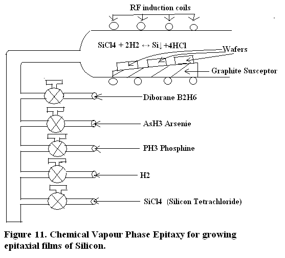
In Figure 11 , we describe CVPD system for obtaining Si Epitaxial Films. A controlled chemical vapour of precise chemical composition at a precisely controlled flow rate is passed over silicon substrates. Si Substrates act as the seed crystals. They are kept at precisely controlled temperature of 1270ºC by RF induction heating hence they are placed on Graphite Susceptors. This gives a precise control of Si molecules, in vapour phase of partial pressure P, impinging upon Si Substrate:
(Impingement Rate) F =


CPVD is suitable for Homo-epitaxy but not for hetero-epitaxy. The byproduct of this reaction is HCl as seen from the chemical equation of reaction:
At 1270ºC SiCl 4 (Silicon Tetrachloride) + 2H 2 ↔ Si↓ +4HCl. 1.
This byproduct HCl can attack the Silicon Substrate and cause chemical etching. Hence Chemical Reaction as depicted Eq.(1) is reversible.
\

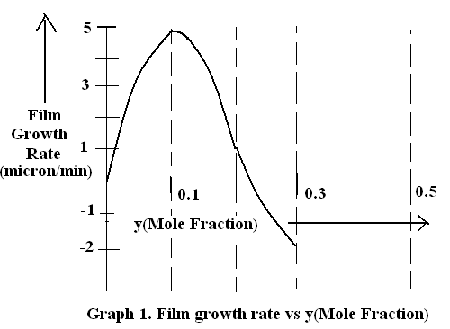
If y(mole fraction = SiCl 4 conc./Total conc) is greater than 0.23 as seen from Graph 1 , growth rate is negative. This means chemical etching of Silicon Wafer. The negative growth rate is used for in-situ cleaning of Silicon Wafers. This is one of the ways of chemical etching while preparing Silicon Wafers from Silicon Ingot.
If y<0.23 we have positive growth rate and Si vapour deposition takes place as an epitaxial film. The growth rate is maximum at y = 0.1 . The maximum growth rate is 5μm/minute.

Notification Switch
Would you like to follow the 'Electrical and electronic materials science' conversation and receive update notifications?