| << Chapter < Page | Chapter >> Page > |
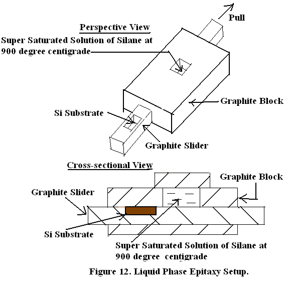
Since CVPD is carried out at 1270ºC, there is the problem of out-diffusion of Arsenic from the substrate into the epitaxial layer. Arsenic is used as buried layer to reduce the series collector resistance of Vertical NPN transistor. Arsenic has very low diffusion coefficient still at the elevated temperature of 1270ºC, some out-diffusion is inevitable. To prevent this out-diffusion altogether, we use Liquid Phase Epitaxy which is shown in Figure 12.
LIQUID PHASE EPITAXY.
The Liquid Phase Epitaxy set up is shown in Figure 12.This is carried out at 900ºC hence the problem of out-diffusion is completely prevented but Silane which is used for LPE is highly toxic. As seen in Figure 12, there is a super saturated solution of Silane kept at 900ºC. By Graphite Slider, the silicon substrate is brought directly underneath the well containing Silane. As Substrate comes in contact with Silane , latter is dissociated into Silicon and Hydrogen and Silicon precipitates onto the substrate forming an epitaxial film on the substrate.

MOLECULAR BEAM EPITAXY
Due to explosive demand of Wireless Communication Equipment there has been a sudden spurt in demand of MBE equipments particularly of multiple wafer MBE equipment which can give a high throughput of epitaxilly prepared wafers.
There are two kinds of epitaxial film growth: Homoepitaxy (same composition) and Heteroepitaxy (different composition). By Molecular Beam Epitaxy, multi-layered thin films of single crystals of different compositions and of atomic dimension can be grown. In effect we can achieve heteroepitaxy which is the hallmark of compound semiconductor devices such as Photonic Devices and GaAs MESFET.
MBE is a process for making compound semiconductor materials with great precision and purity. These materials are layered one on top of the other to form semiconductor devices such as transistors and lasers. These devices are used in such applications as fiber-optics, cellular phones, satellites, radar systems, and display devices. MBE is used for fabrication of Super-lattices and hetero-junction MESFET. Super lattices are periodic structures of alternating Ultra-thin layers of compound semiconductor.
MBE growth produces complex structures of varying layers which are further processed to produce a range of electronic and optoelectronic devices, including high speed transistors, light-emitting diodes, and solid state lasers. MBE is a powerful technique both for research into new materials and layer structures, and for producing high-performance devices.

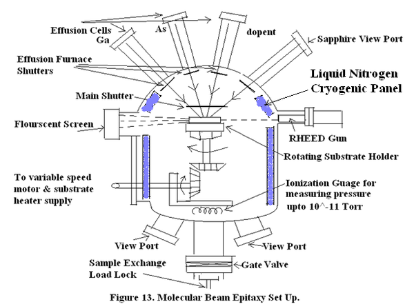
Referring to Figure 13:
The walls of the chamber cooled with liquid nitrogen. This cryogenic screening around the substrate minimizes the spurious flux of contaminating atoms and
Sample Exchange Load Lock-this permits maintenance of Ultra High Vacuum while changing the substrate.
Effusion Cells- this contains the solid source to be evaporated and deposited on the substrate. Temperature of the effusion oven is adjusted to give desired evaporation rate.
Rotating Substrate Holder- rotation of substrate ensures less than ±1% doping variation and ±0.5% in thickness variation.

Notification Switch
Would you like to follow the 'Electrical and electronic materials science' conversation and receive update notifications?