| << Chapter < Page | Chapter >> Page > |

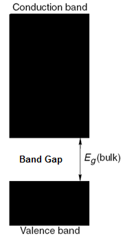
The electronic structure of any material is given by a solution of Schrödinger equations with boundary conditions, depending on the physical situation. The electronic structure of a semiconductor ( [link] ) can be described by the following terms:

By the solution of Schrödinger’s equations, the electrons in a semiconductor can have only certain allowable energies, which are associated with energy levels. No electrons can exist in between these levels, or in other words can have energies in between the allowed energies. In addition, from Pauli’s Exclusion Principle, only 2 electrons with opposite spin can exist at any one energy level. Thus, the electrons start filling from the lowest energy levels. Greater the number of atoms in a crystal, the difference in allowable energies become very small, thus the distance between energy levels decreases. However, this distance can never be zero. For a bulk semiconductor, due to the large number of atoms, the distance between energy levels is very small and for all practical purpose the energy levels can be described as continuous ( [link] ).
From the solution of Schrödinger’s equations, there are a set of energies which is not allowable, and thus no energy levels can exist in this region. This region is called the band gap and is a quantum mechanical phenomenon ( [link] ). In a bulk semiconductor the bandgap is fixed; whereas in a quantum dot nanoparticle the bandgap varies with the size of the nanoparticle.
In bulk semiconductors, since the energy levels can be considered as continuous, they are also termed as energy bands. Valence band contains electrons from the lowest energy level to the energy level at the lower edge of the bandgap ( [link] ). Since filling of energy is from the lowest energy level, this band is usually almost full.
The conduction band consists of energy levels from the upper edge of the bandgap and higher ( [link] ). To reach the conduction band, the electrons in the valence band should have enough energy to cross the band gap. Once the electrons are excited, they subsequently relax back to the valence band (either radiatively or non-radiatively) followed by a subsequent emission of radiation. This property is responsible for most of the applications of quantum dots.
When an electron is excited from the valence band to the conduction band, corresponding to the electron in the conduction band a hole (absence of electron) is formed in the valence band. This electron pair is called an exciton. Excitons have a natural separation distance between the electron and hole, which is characteristic of the material. This average distance is called exciton Bohr radius. In a bulk semiconductor, the size of the crystal is much larger than the exciton Bohr radius and hence the exciton is free to move throughout the crystal.

Notification Switch
Would you like to follow the 'Nanomaterials and nanotechnology' conversation and receive update notifications?