| << Chapter < Page | Chapter >> Page > |
The components you have been learning about so far — resistors, capacitors and inductors — are called passive components. They do not change their behaviour or physics and therefore always have the same response to changes in voltage or current. Active components are quite different. Their response to changes in input allows them to make amplifiers, calculators and computers.
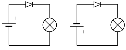
A diode is an electronic device that allows current to flow in one direction only.

A diode consists of two doped semi-conductors joined together so that the resistance is low when connected one way and very high the other way.

A full explanation of diode operation is complex. Here is a simplified description. The diode consists of two semiconductor blocks attached together. Neither block is made of pure silicon — they are both doped . Doping was described in more detail in Section 10.3.
In short, p-type semiconductor has fewer free electrons than normal semiconductor. `P' stands for `positive', meaning a lack of electrons, although the material is actually neutral. The locations where electrons are missing are called holes . This material can conduct electricity well, because electrons can move into the holes, making a new hole somewhere else in the material. Any extra electrons introduced into this region by the circuit will fill some or all of the holes.
In n-type semiconductor, the situation is reversed. The material has more free electrons than normal semiconductor. `N' stands for `negative', meaning an excess of electrons, although the material is actually neutral.
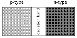
When a p-type semiconductor is attached to an n-type semiconductor, some of the free electrons in the n-type move across to the p-type semiconductor. They fill the available holes near the junction. This means that the region of the n-type semiconductor nearest the junction has no free electrons (they've moved across to fill the holes). This makes this n-type semiconductor positively charged. It used to be electrically neutral, but has since lost electrons.
The region of p-type semiconductor nearest the junction now has no holes (they've been filled in by the migrating electrons). This makes the p-type semiconductor negatively charged. It used to be electrically neutral, but has since gained electrons.
Without free electrons or holes, the central region can not conduct electricity well. It has a high resistance, and is called the depletion band . This is shown in [link] .

You can explain the high resistance in a different way. A free electron in the n-type semiconductor will be repelled from the p-type semiconductor because of its negative charge. The electron will not go into the depletion band, and certainly won't cross the band to the p-type semiconductor. You may ask, “But won't a free electron in the p-type semiconductor be attracted across the band, carrying a current?” But there are no free electrons in p-type semiconductor, so no current of this kind can flow.

Notification Switch
Would you like to follow the 'Siyavula textbooks: grade 12 physical science' conversation and receive update notifications?