| << Chapter < Page | Chapter >> Page > |
7.6.2.1. Calculation of Standard Unit of Capacitance □C g
Generally while designing we donot work in terms of absolute values of capacitances. Instrtead we work in relative terms with repect to some standard value and the absolute value of that standard is recorded accurately.
In the present case the gate-to-channel capacitance of a MOS transistor with W=L=2λ is calculated fot the different generations of technology and this is refered to as □C g . Table 7.6.3 gives the values of □C g for three generations of technology namely 5μm, 2μm and 1.2μm.
Table 7.6.3. Standard Unit of Capacitance for 5μm, 2μm and 1.2μm Generation.
| 5μm | 2μm | 1.2μm | |
| Gate-to-Channel | 4 pF×10 -4 /μm 2 | 8 pF×10 -4 /μm 2 | 16 pF×10 -4 /μm 2 |
| □C g | (5μm×5μm)×4 pF×10 -4 /μm 2 = 0.01 pF | (2μm×2μm)×8 pF×10 -4 /μm 2 = 0.0032 pF | (1.2μm×1.2μm)×16 pF×10 -4 /μm 2 = 0.0023 pF |
In Table 7.6.4 the oxide thickness is given for different Generations of Technology.
Table 7.6.4 Oxide Thickness scaling with channel length scaling.
| L | 5 μm | 2 μm | 1.2 μm | 90nm | 45nm | 30nm |
| D | 88nm | 44nm | 22nm | 1.3nm=5atomic layers |
As oxide becomes thinner, current leakage through the oxide layer by means of quantum tunneling and consequent heating becomes a serious problem. We need physically thick oxide to prevent the leakage and electrically thin to keep the threshold Voltage low. Rewriting Eq 7.6.2.1 we get:

By inspection of the above Equation we see that if relative permittivity is doubled in the numerator then thickness of the oxide layer,D, will also double thus making the Gate dielectric layer thick enough to prevent leakage aand leaving the threshold voltage unaffected.
Along with vertical scaling, lateral scaling has taken place. This has led to reduction in cross-sevtional area ‘A’. This decreases Capactance C and increases threshold voltage.. If threshold voltage has to be maintained around 0.5V then the thickness D will once again have to be decreased.
Therefore High K-metal gate was introduced. High K made the oxide layer thicker and metal gate prevented Fermi level pinning..
7.6.2.2. Metal 1 to Substraate Area Capacitance Calculation for 5μm Generation.
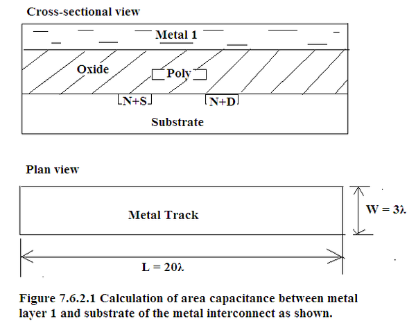
In Figure 7.6.2, the cross-sectional view and the plan view of a metal interconnect is shown.
The length by breadth of the metal track =(L=20λ×W=3λ) is given. Determine Metal 1 to Substrate area capacitance in terms of the standard capacitance.
From Table 7.6.1, for 5μm Generation of CMOS:
Metal 1 to substrate capacitance per unit area = 0.075×□C g
Therefore total area relative capacitance :

Therefore Total area capacitance between metal 1 and substrate
=15×0.075×□C g = 1.125□C g
The absolute value of the interplate capacitance
between metal 1 and substrate=1.125×0.01pF=0.0125pF.
Similarly same area between poly-Si and substrate= 15×0.1×□C g =1.5□C g ;
Same area between n-type diffusion and substrate =15×0.25×□C g =3.75□C g ;

7.6.2.3 Capacitance calculation in multi layer structures.
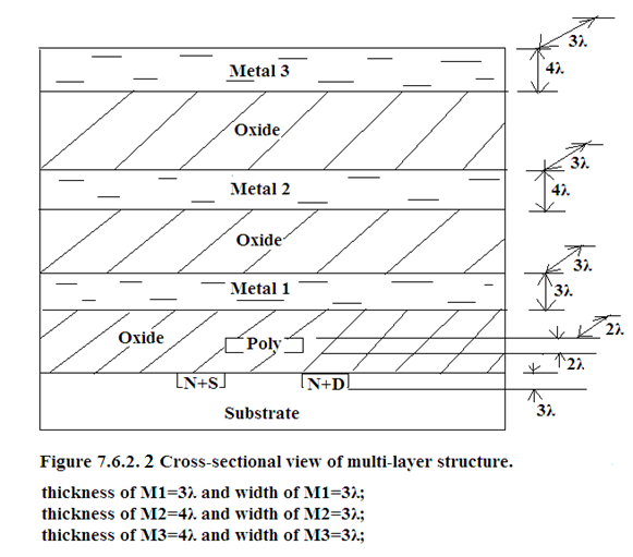
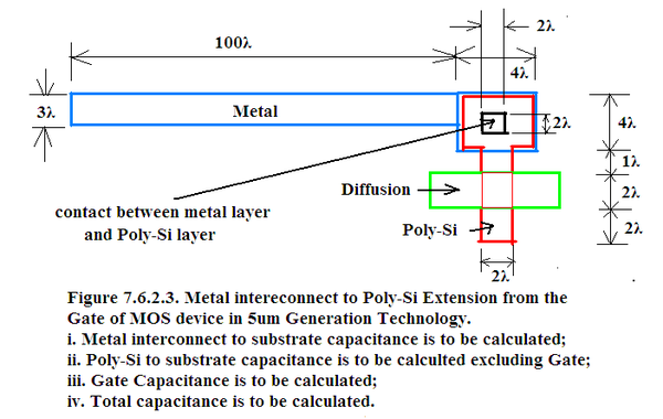
A CMOS IC with multi-layer metal interconnect is shown in Figure 7.6.2.2 and in Figure 7.6.2.3. plan view of metal interconnect making contact with Poly-Si extension from the gate is shown.
It should be noted that Poly-Si over the Gate lies over 88.5nm thin oxide layer has the nomenclature of Gate-to-Chanel and has the standard value of 1□C g on the other hand
Poly-Si over the remaining portion runs over 5μm thick oxide layer and has the nomenclature Poly-Si-to-Substrate and has the value of 0.1□C g .

In Figure 7.6.2.3 we are required to determine Metal interconnect-to-Substrate capacitancve, Poly-Si-to-Substrate capacitance excluding Gate, Gate capacitance and total capacitance are to be calculated.
Relative area of metal interconnect with respect to standard capacitance =(100λ×3λ)/(2λ×2λ) = 75
Therefore Metal interconnect-to-Substrate Capacitance = 75×0.075□C g = 5.625□C g ;
C m = 5.625□C g ;
Poly-Si-to-Substrate Capacitance(excluding Gate area)
=[(overlap area + extension area of Poly-Si excluding Gate)/(2λ×2λ)]×0.1□C g
=[(4λ×4λ +3λ×3λ)/ 2λ×2λ)]×0.1□C g =0.55□C g ;
C poly = 0.55□C g ;
C gate = 1□C g ;
Therefore C total = C m + C poly + C gate =(5.625+0.55+1) □C g = 7.175□C g ;
The absolute value is C total = 7.157×0.01pF=0.0717pF for 5μm Generation.


Notification Switch
Would you like to follow the 'Solid state physics and devices-the harbinger of third wave of civilization' conversation and receive update notifications?