| << Chapter < Page | Chapter >> Page > |
M= Avalanche Multiplication Factor which does not come into picture at low voltages.
Initially α F is very small due to very low currents flowing through it but as V AK (voltage between anode and cathode) increases, due to shrinking of Base width both alphas improve.
At α F1 + α F2 = 1, the current increases in a runaway fashion only limited by the external resistance. This is the firing point of the parasitic SCR embedded in the CMOS structure and can do irreversible damage to the IC.
7.3.16.2. How does the runaway process of SCR current set in?
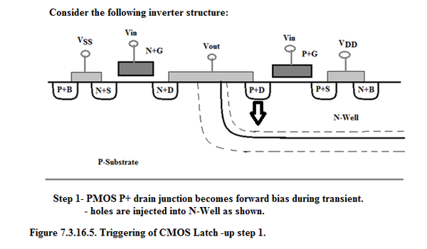
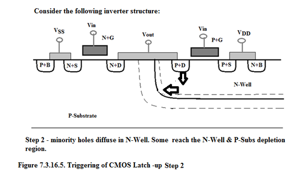
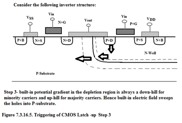
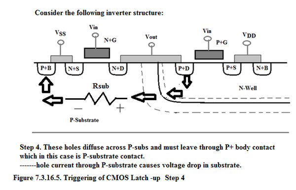
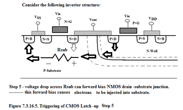
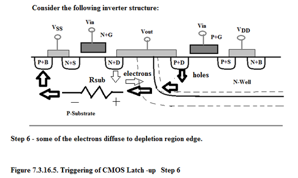
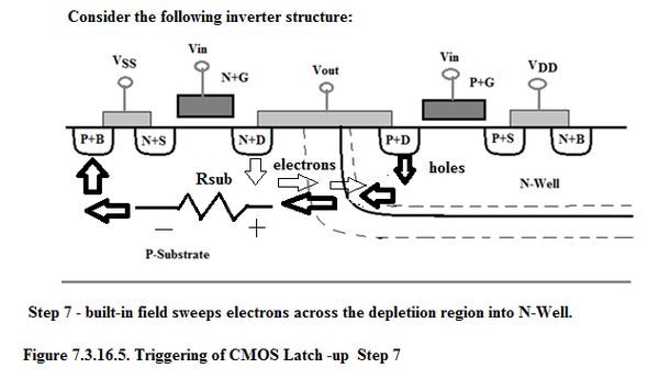
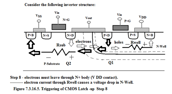
As we see in Figure 7.3.16.5. Step 8 a positive feed back loop or regenerative loop is set up.
A transient at P+Drain of PMOS sets up a hole current through Rsub which triggers N+drain of NMOS to set up an electron current through Rwell.
The electron current through Rwell further enhances hole current through Rsub and hole current through Rsub further increments the electron current through Rwell. This leads to a runaway condition which results in a large current flow from V DD bus to V SS bus and subsequently damages the CMOS structure.
7.3.16.3. The remedies of Latching Problem in N-Well process/P-Well process.
Design approach.(internal implants and larger spacing)
As we see in Figure 7.3.16.5. Step 8, we have two BJTs Q1 and Q2.
Q1 is comprised of P+(drainof PMOS)-Nwell-Psubstrate and Q2 is comprised of N+(drain of NMOS)-Psubstrate-Nwell.
Q1 current gain can be reduced by introducing a buried layer in N-Well. This reduces the injection efficiency.
Q2 current gain can be reduced by increasing the spacing between N-Well and N+ Source/Drain. Increase in the spacing leads to reduced Base Transport Factor.
Fabrication approach.
As we saw in our discussion, Rsub and Rwell play a crucial role in setting up the runaway process. If by chosing higher doping level we reduce Rsub and Rwell then also runaway process will be prevented
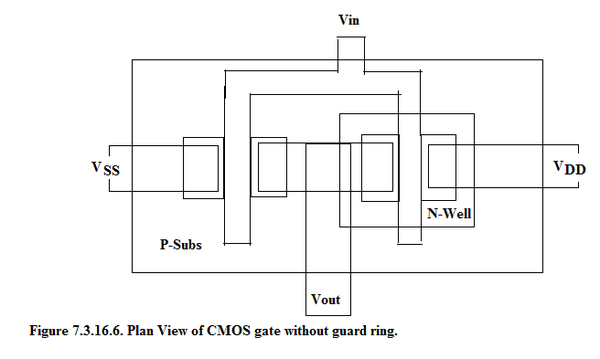
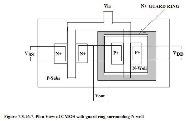
Guard rings around N-Well with frequent contacts to the rings reduces the parasitic resistances. This also prevents the latch-up. The CMOS layout plan view is shown in Figure 7.3.16.6 and in Figure 7.3.16.7. without and with guard ring respectively.
7.3.16.4. Prevention of Latching in Twin-Tub Process.
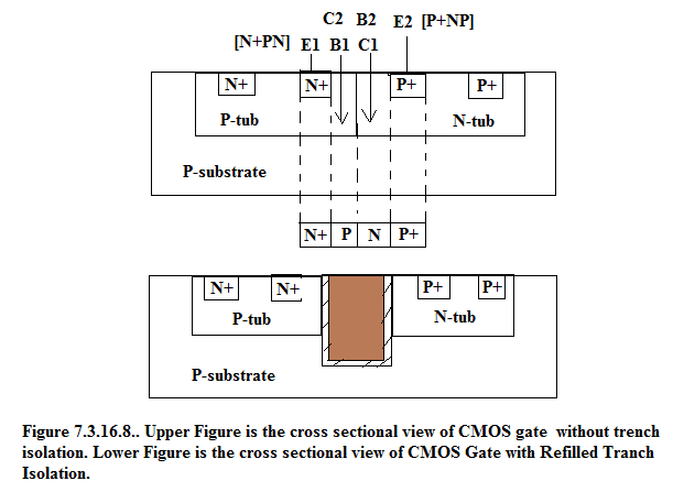
In Twin-Tub process by the formation of ‘Refilled Trench Isolation’ between Twin Tub.This isolation prevents formation of parasitic BJT as shown in Figure 7.3.16.8.
The trench is formed in Silicon Substrate by anisotropic reactive sputter etching. Oxide layer is grown on the side-walls and bottom of the trench. This oxide lined trench is filled by Poly-Si or SiO 2 . This kind of structure is shown in Figure 7.3.16.8.
The trench isolation disrupts the parasitic BJT hence parasitic SCR is prevented structurally as shown in Figure 7.3.16.8
7.3.16.5. BiCMOS Latch-up susceptibility.
BiCMOS is less susceptible to latch-up problems because it has less substrate body resistance (Rsub) and less n-well body resistance (Rwell). Hence it requires larger currents through Rsub and Rwell to trigger latch-up process.
A typical BiCMOS in N-well process is shown in Figure 7.3.16.9
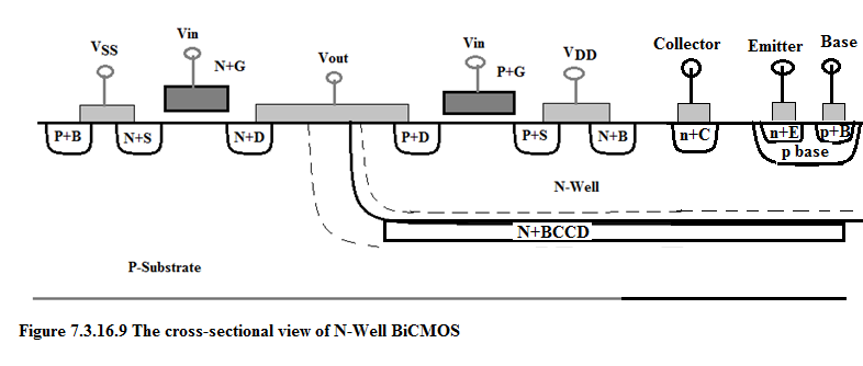
As can be seen from Figure 7.3.16.9 there is parasitic vertical PNP transistor constituted of
P base, N-Well and Psubstrate. This is a part of the N-Well Latch-up circuit. Due to the presence of N+BCCD(buried N+ subcollector), the life-time of minority carriers in the base of the parasitic vertical PNP is reduced. This reduces beta of the vertical PNP transistor since beta = life-time of minority cariers/ transit time. Hence latch-up susceptibility is reduced.

Notification Switch
Would you like to follow the 'Solid state physics and devices-the harbinger of third wave of civilization' conversation and receive update notifications?