| << Chapter < Page | Chapter >> Page > |
PMOS Tuning
PMOS devices are a special case since the boron doped Source/Drain implants overall tend to absorb interstitials rather than emit them. The reverse short channel effect in buried channel PMOS devices can be caused by high angle implants. If high angle implants are used, the reverse short channel effect can be tuned using the LAT.RATIO1 parameter in the IMPLANT statement.
7.8.5: Related Issues on using the Device Simulator ATLAS for MOS Process Tuning
It should now be known that calibrating an ATHENA process file involves using the device simulator ATLAS to a significant extent. Hence, it’s imperative that the use of the device simulator doesn’t create additional errors, rendering the process calibration results invalid.
Fortunately, the device physics involved in simulating the conditions required to extract a threshold voltage are not demanding. The drain voltage required to extract a threshold voltage is only 50-100mV so effects such as impact ionization can be neglected. The field perpendicular to the gate is also relatively low around the threshold voltage so field effects in this direction will do little effect. We recommend, however, using at least the models SRH and CVT during the calculation. Other parameters for silicon are sufficiently well known for silicon to the point that the results from the device simulator are reliable.
The first important point is to ensure that you let the device simulator calculate the work function of the gate electrode from the simulated doping profile rather than assigning a value to it. This means, making sure that the polysilicon gate is not itself defined as an electrode but rather a layer of metal, usually aluminum, is deposited on top of the polysilicon gate. Therefore, this metal layer is the film defined as the electrode. Do not assign a work function to this deposited metal electrode to ensure that it behaves as an ohmic contact rather than a Schottky contact. The effective work function of the poly gate will then be correctly calculated from the doping profile in the polysilicon.
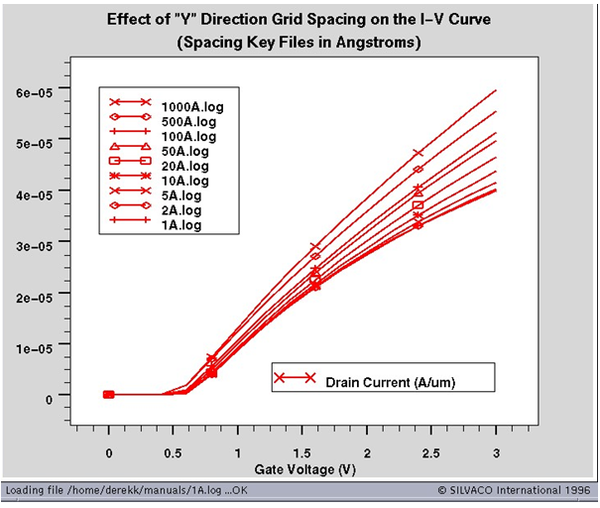
An important area for accuracy in MOSFETs is modeling the inversion region under the gate. As it is, this charge that is responsible for current conduction in the device. The inversion region charge under the gate-only extends approximately 30 Angstroms into the silicon. The inversion region charge density under the gate falls off rapidly with depth into the silicon. It is imperative that there are several mesh points in the Y direction in this inversion region to model the drain current correctly. Accordingly, we recommend that the mesh spacing under the gate be no more than 10 Angstroms (1 nm).
You would think that a 10 Angstrom mesh under the gate would result in a huge number of mesh points. But, there only needs to be approximately three mesh points within the inversion region in the Y direction. The grid spacing can increase rapidly in spacing away from the oxide-silicon interface.
Figure 7.43 shows the effects of changing the mesh spacing at the interface on the simulated drain current. You can see from this figure that too coarse of a mesh always results in too high of a current simulated.

Figure 7.43: The effect of changing the mesh spacing at the interface on the simulated drain current
If contact resistance is a problem, then include it in the CONTACT statement. The resistance added to the CONTACT statement should be the measured resistance per contact divided by the number of contacts on each individual electrode. Obviously for D.C. measurements, the resistance on the gate contact will have no effect on the results since no current flows in this direction.
Checking the Predictive Powers of Tuned Process Parameters
If the process simulation has been correctly tuned, the process and device simulators should have predictive powers. To check the validity of the tuning process, use a new set of electrical data that was not used during the tuning process. For example, a good alternative set of data is to check the threshold voltage versus gate length for a non-zero voltage applied to the MOSFET body contact.
Conclusion
Using just one set of easily obtained measured electrical data, namely a plot of threshold voltage versus gate length, you can obtain most of the tuning parameters required for accurate process simulation. The other most important piece of data required is an accurate measurement of the gate oxide thickness, which is routinely measured in any instance.
You have been given specific advice as to which process and device models to use for each process in order to get the best results out of the simulation software. In particular, the correct use of models for the implantation and diffusion processes is stressed, as this has a dramatic effect on MOSFET characteristics, especially as anneal times and device dimensions decrease.

Notification Switch
Would you like to follow the 'Solid state physics and devices-the harbinger of third wave of civilization' conversation and receive update notifications?