| << Chapter < Page | Chapter >> Page > |

Since the resistors are more or less temperature tracked therefore ratios remain temperature independent. Hence output voltage V o does not vary with temperature. Only mismatch in the input circuit (with respect to beta, V BE , I CO ) causes a finite V o (i.e. offset voltage), and with temperature variation this mismatch gates magnified and causes a drift of V 0
In Fig 6.26 it is seen that output transistor Q 12 and Q 13 have three times cross-sectional area as that of the emitter base junction of D4. Hence output transistors carry 3 times as much current as D4. From dc bias condition,
I Q12 = I Q13 = 3(I D4 ) = 308mA;
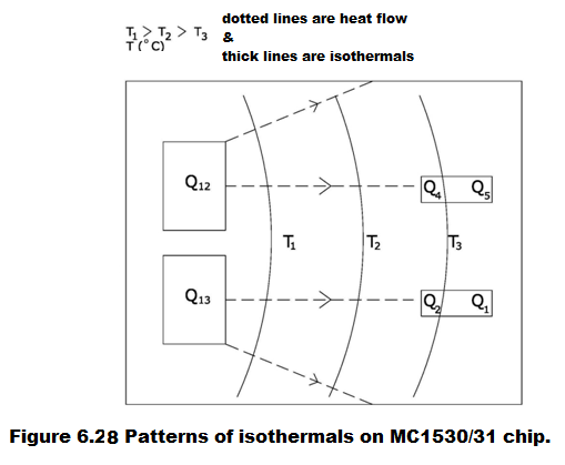
Because of this enhanced signal handling capacity MC1530 will drive load resistors as low as 1k to a maximum p-p swing of 11 volts with Vcc = ±6 volts. Also because of high quiescent current in output stage maximum power is dissipated in Q12, Q13. Most of the dissipated energy is sunk by the header but not without heating the chip. Hence during the operation invariably a temperature gradient and a set of isothermals are set up on the chip as shown in Fig (6.28).

As can be seen in Fig.(6.28) input pairs Q 2 and Q 4 , Q 1 and Q 5 are kept on the least isothermal, farthest away from the output transistors, and in close vicinity to each other. The result is that there is least heating of the input pairs because of high output power dissipation, maximum temperature tracking of the input pairs and diffusion profiles of the input pairs very closely match to one another. Because of close proximity and the resultant diffusion profile matching, V BE and betas of the input pairs of transistors very closely match hence very low input offset voltages and currents are caused typically V os =2mV. Because of excellent temperature tracking of the input pairs, the long term drift of temperature appears mainly as common mode signal thereby minimizing the long term drift of V os to 3.8µV/ o C. Both these parameters V os and low drift are indicative of proper layout of the devices on the chip.
As can be seen in Fig.(6.27) D 1, D 2 are in close proximity to Q 3 and the three are more or less on the same isothermal, D 3 is in close proximity to Q 10 as well as the two are on same isothermal, and D 4 is in close proximity to Q 13 . Each of these are bias current sources. Because of matching of the characteristics and because of temperature tracking of the devices in the current sources, each current source is the current mirror of the reference current. And because of the use of diode configuration of the transistor which results in heavy voltage shunt feedback the reference current are highly stabilised against temperature changes. This is also known as diode compensation. Hence almost drift free near ideal current sources are achieved. Because of the stability the bias sources, the ac performance of this chip is highly stabilised. The open loop gain A d = 72dB ± 1.5dB from T = -55 o C to T= +125 o C.
The monolithic IC chip MC 1530-31 is mounted on 10 pins TO-5 packages. Two battery biases V cc ,
-V EE , output and ground leads require four pins, two pins are used for inputs and four pins are for internal connections.

Notification Switch
Would you like to follow the 'Solid state physics and devices-the harbinger of third wave of civilization' conversation and receive update notifications?