| << Chapter < Page | Chapter >> Page > |

Tailoring the band-gap by finely tuning the stoichiometric coefficient ‘y’ is known as Band-Gap Engineering . In the process of Band-Gap Engineering, the lattice parameter is also reduced from 5.65Angstrom for GaAs to 5.5Angstrom for GaP. We can use the relation ship (5.5.2) to determine the constituent materials and the substrate for fabricating LEDS of different colours namely Red, Orange, Yellow, Green and Blue. The results of thgis design is given in Table 5.5.1.
Red LED corresponds to 0.64μm which can be emitted from GaAs (1-y) P y of E g =1.9eV. The substrate used is GaAs and stoichometric coefficient ‘y’=0.4.
Orange LED corresponds to 0.62μm which can be emitted from GaAs (1-y) P y of E g = 2.0eV. The substrate used is GaP and stoichometric coefficient ‘y’=0.5.
Yellow LED corresponds to 0.58μm which can be emitted from GaAs (1-y) P y of E g =2.14eV. The substrate used is GaP and stoichometric coefficient ‘y’=0.58.
Green LED corresponds to 0.55μm which can be emitted from GaAs (1-y) P y of E g =2.35eV. The substrate used is GaP and stoichometric coefficient ‘y’=0.656.
Blue LED corresponds to 0.475μm which can be emitted from GaAs (1-y) P y of E g =2.61eV. The substrate used is SiC and stoichometric coefficient ‘y’=0.9.
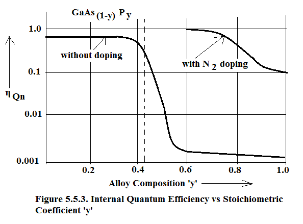
Generally compound semi-conductors have direct band-gap and hence have high Internal Quantum Efficiency. But in ternary GaAs (1-y) P y as ‘y’ exceeds 0.45, the ternary compound becomes In-direct and its Internal Quantum Efficiency drastically falls as shown in Figure 5.5.3.By doping this material with Nitrogen it is transformed into Direct Band-Gap material and internal Quantum efficiency is restored but it is not good enough for LASER Diodes.
By Nitrogen doping , traps are introduced vertically above the valence band peak in E-p or E-k diagram. These traps enable vertical transitions thereby improving internal Quantum Efficiency.

Section 5.5.2.Homo-Junction, Hetreo-Junction and Double Hetero-junction.
Homojunctions are made of the same semiconductor material on both sides of the junction. Whereas Heterojunction are made of different band-gap material, but matching lattice parameters, on both sides of the junction. In Double Heterojunction one material of narrow bandgap is sandwitched between two other materials of wider bandgap. This leads to the formation of Quantum Well in the narrow bandgap material.
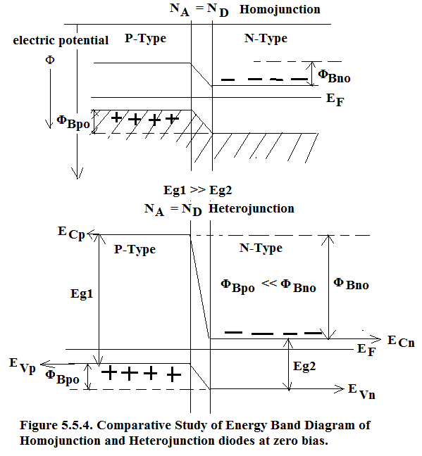
In a symmetric Homojunction , diode current is equally divided between electrons and holes and Injection Efficiency in any direction is 0.5. But in symmetric Heterojunction (symmetric in doping sense but highly asymmetric in Band Gap sense) , diode current is very unequally divided between electrons and holes as will become clear from Figure 5.5.4.
As seen in Figure 5.5.4. in Homojunction Diode with equal doping, the built-in Barrier potential seen by electrons on N-Side is the same as that seen by holes on P-Side. This is because Φ Bno = Φ Bpo . But in Heterojunction Diode (with very unequal Energy Band Gap) even with equal doping, Φ Bno ≠ Φ Bpo . In Figure 5.5.4., Band Gap on P-Side (E g1 ) is much larger than Band Gap on N-Side (E g2 ). Hence Φ Bno >Φ Bpo . This means injection from P-Side is several orders of magnitude larger than the injection from N-Side. Hence Injection Efficiency is almost 100% from P-Side.
This becomes evident if we look at the Injection Efficiency Expression. From Equation 4.3.13:

For equal Homojunction:

If Emitter Band Gap>>Base Band Gap then:

This proves that in Heterojunction diode there is a copious injection of majority carriers from Large Band Gap Material to Narrow Band Gap Material. This will help achieve much more efficient and more powerful LEDs as well as LASER Diodes.

Section 5.5.3. Double Heterojunction LED
Homojunction LED suffer from poor internal quantum efficiency and considerable loss of radiated photons. These problems are considerably over-come by Double Heterojunction LED.
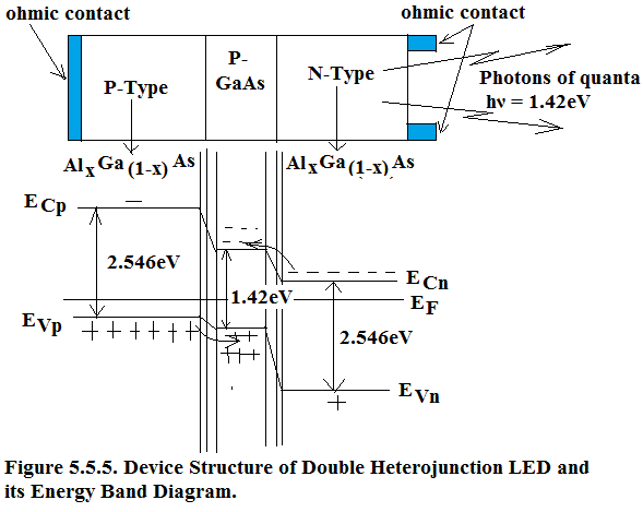
As seen in Figure 5.5.5. P-Type lightly doped GaAs(Band-Gap=1.42eV) is sandwitched between two large band-gap layers of AlGaAs(Band-Gap=2.546eV).
In AlGaAs, Al and Ga are in Group III and As is in Group V. By controlling the stoichiometric coefficient ‘x’ in Al X Ga (1-X) As, the band-gap can be tailored according to the requirement.

At x = 0.9, the band-gap of Al X Ga (1-X) As is 2.546eV.

As we see in Figure 5.5.5., a narrow band gap layer(GaAs, 1.42eV) is confined or sandwiched between two wide band gap layers(AlGaAs,2.546eV). In effect a thin quantum well is created in the middle layer. This causes heavy injection of holes from the P-Type layer on the left and heavy injection of electrons from N-Type on the right. So a large amount of electrons and holes are confined in this narrow quantum well leading to rapid direct radiative recombination.
His has three distinct advantages over Homojunction Surface Emitting LED.
These four factors greatly improve the external as well as internal Quantum Efficiency. The Quantum Well comprises of 0.1 to 0.2μm thick narrow band-gap material. These surface emitting structures and edge emitting structures(not described here) are particularly useful in improving the coupling efficiency with te optical fibers.

Notification Switch
Would you like to follow the 'Solid state physics and devices-the harbinger of third wave of civilization' conversation and receive update notifications?