| << Chapter < Page | Chapter >> Page > |
SSPD_Chapter 5_Section 5.3. Spectal Responsivity of Photo-Diodes.
Spectral Responsivity is the main parameter which decides the application of Photo-diodes of given Spectral Responsivity curves. Here we analyze the theoretical formulation of this parameter and then we study the design of Photo-Diodes for various applications.
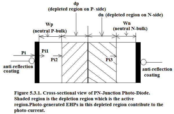
Electron-Hole Pairs (EHPs) generated in the neutral bulk travel by diffusion whereas EHPs generated in depleted region travel by drift. As shown below diffusion velocity is two orders of magnitude smaller than the drift velocity:


Therefore:

Hence bulk generated EHP slow down the photo-response. Therefore contribution of bulk-generated EHPs to photo-current is kept at the minimum. The depleted region of the reverse biased diode is kept at the maximum and is kept as the active contributor of the photo-current.
For theoretical formulation of the Spectral Responsivity let us examine Figure 5.3.1.

The intervening Bulk Region always brings down the effective absorption of the incident light. To ensure that all the incident quanta get absorbed, we use anti-reflection coating on the front surface of the photo-diode and we minimize the neutral bulk region widths.
Let internal quantum efficiency = η (no. of EHPs generated per photon).
Ideally 100photons should generate 100EHPs and this implies η =1 but practically η<1.


Each EHP gives rise to ‘q’ coulombs of circuital charge hence effective photo-generated current is:

Now spectral Responsivity is defined as:

In Equation 5.3.8. there is no threshold term as predicted by Equation 5.1. Hence Equation 5.3.8. gives the dotted curve in Figure 5.3.2. which is an idealized Spectral Responsivity curve. The real Responsivity Curve is given by Bold Curves. Table 5.3.1. tabulates the coordinates of the idealized curves for different photo-diodes[(λ Threshold =1000nm, η=0.9), (λ Threshold =1500nm, η=0.5), (λ Threshold =1700nm, η=0.7),]
Table 5.3.1. Responsivity data(A/W) for 3 Photo-Diodes of given λ Threshold &η.
| λ(cm) | 500×10 -7 | 600×10 -7 | 700×10 -7 | 900×10 -7 | 1000×10 -7 | 1500×10 -7 | 1900×10 -7 | λ Threshold |
|---|---|---|---|---|---|---|---|---|
| R(η=0.9) | 0.36 | 0.435 | 0.508 | 0.653 | 0.725 | 1.09 | 1.38 | 1000nm |
| R(η=0.5) | 0.202 | 0.242 | 0.2823 | 0.363 | 0.403 | 0.605 | 0.766 | 1500nm |
| R(η=0.7) | 0.2823 | 0.339 | 0.395 | 0.508 | 0.5646 | 0.846 | 1.073 | 1700nm |

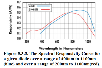
Experimental curves for a given photo-diode (λ Threshold =1000nm, η=0.8) are given in Figure 5.3.3. over a spectral range of 400nm to 1100nm(blue curve) and over a range of 200nm to 1100nm(red curve). As can be seen in Figure 5.3.2. as well as in Figure 5.3.3. the Spectral Responsivity Curve sharply dips in the region of threshold wavelength(λ Thrshold ) given by Equation 5.1. as expected. At longer wavelengths the photons are not energetic enough to cause photo-excitation.
In Figure 5.3.2. at shorter wavelengths also there is departure from the idealized curve. At shorter wavelengths , absorption coefficient (α) sharply increases as seen in Figure 5.2. Hence penetration depth becomes shallow which leads to reduced absorbed power resulting in reduced response. But in Figure 5.3.3. in UV region the curve experiences a bump instead of a dip. This point s not clear to me at this point.
5.4. Design of a Photo-Diode in different parts of the Electro Magnetic Spectrum depending on the application.
Different applications require maximal response in different parts of SPECTRUM. For instance Night vision requires maximum response in Near IR(800nm to 1000nm).
5.4.1. PIN Diode.
For maximal response of the photo-diodes in faintest of light, various structural modifications are adopted. The first modification is the introduction of intrinsic region between P and N region. As seen in Figure 5.4.1. a PIN diode has a depletion region in the entire Intrinsic Region. This gives a direct control over the depletion region and the active region can be tailored according to our requirements.
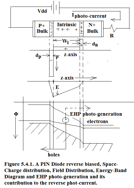
As seen in Figure 5.4.1. the active layer comprises of W active = d p +W i +d n .This increase in active layer by the addition of intrinsic layer increases the responsivity mani-fold. Also the large drift field through out the intrinsic region is effective in quickly removing the photo-generated EHPs. This adds to the speed of the response of the photo-diode.
5.4.2. Avalanche Photo-diode (APD) or Reach Through Avalanche Photo-diode.
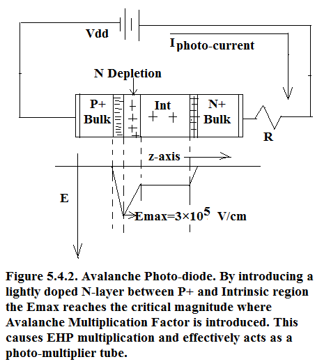
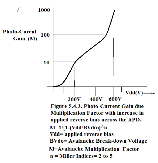
As seen in Figure 5.4.2., a fourth layer of lightly doped N-layer considerable increases the Emax and it crosses the critical field and introduces Avalanche Multiplication Factor (M). This effectively multiplies the photo-current as it did in photo-multiplier tube in Vacuum Tube Era but it introduces considerable amount of noise due to the statistical nature of Avalanche Multiplication. This Noise can be suppressed by making the ionization rate due to Electron and Hole vastly unequal.
In a Si-APD it is possible to make electron ionization rate = 100 times hole ionization rate. This considerable suppresses the Multiplication Noise.
In Ge, GaAs and in InGaAS we have electron ionization rate = 10 times hole ionization rate hence here there is considerable noise and hence it cannot operate in very faint light environment.
The Photo-current multiplication graph is shown in Figure 5.4.3.

Notification Switch
Would you like to follow the 'Solid state physics and devices-the harbinger of third wave of civilization' conversation and receive update notifications?