| << Chapter < Page | Chapter >> Page > |

A common problem seen in AFM images is the presence of artifacts which are distortions of the actual topography, usually either due to issues with the probe, scanner, or image processing. The AFM scans slowly which makes it more susceptible to external temperature fluctuations leading to thermal drift. This leads to artifacts and inaccurate distances between topographical features.
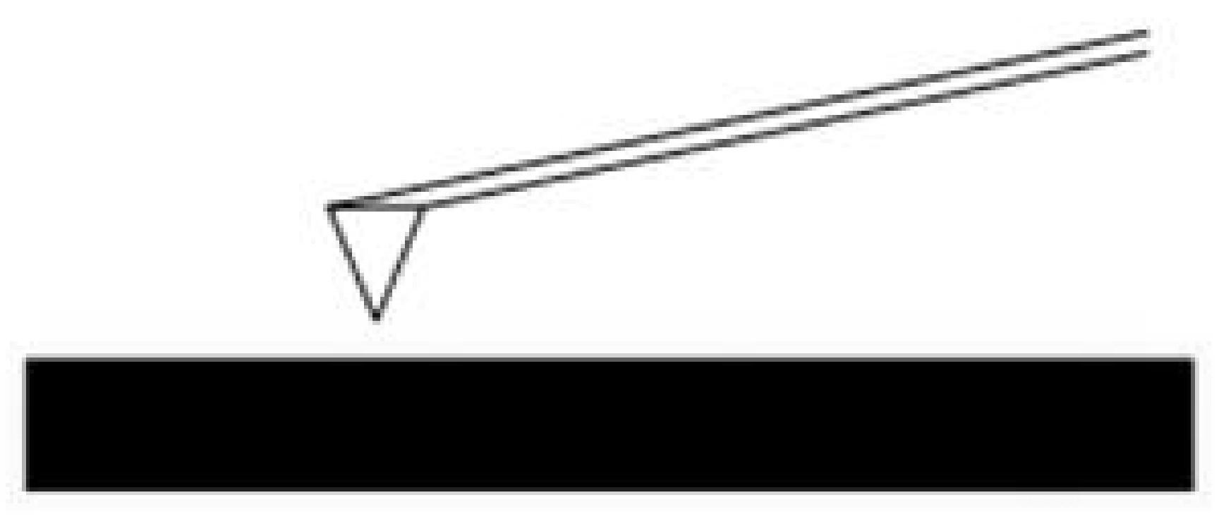
It is also important to consider that the tip is not perfectly sharp and therefore may not provide the best aspect ratio, which leads to a convolution of the true topography. This leads to features appearing too large or too small since the width of the probe cannot precisely move around the particles and holes on the surface. It is for this reason that tips with smaller radii of curvature provide better resolution in imaging. The tip can also produce false images and poorly contrasted images if it is blunt or broken.
The movement of particles on the surface due to the movement of the cantilever can cause noise, which forms streaks or bands in the image. Artifacts can also be made by the tip being of inadequate proportions compared to the surface being scanned. It is for this reason that it is important to use the ideal probe for the particular application.
The sample size varies with the instrument but a typical size is 8 mm by 8 mm with a typical height of 1 mm. Solid samples present a problem for AFM since the tip can shift the material as it scans the surface. Solutions or dispersions are best for applying as uniform of a layer of material as possible in order to get the most accurate value of particles’ heights. This is usually done by spin-coating the solution onto freshly cleaved mica which allows the particles to stick to the surface once it has dried.
AFM is particularly versatile in its applications since it can be used in ambient temperatures and many different environments. It can be used in many different areas to analyze different kinds of samples such as semiconductors, polymers, nanoparticles, biotechnology, and cells amongst others. The most common application of AFM is for morphological studies in order to attain an understanding of the topography of the sample. Since it is common for the material to be in solution, AFM can also give the user an idea of the ability of the material to be dispersed as well as the homogeneity of the particles within that dispersion. It also can provide a lot of information about the particles being studied such as particle size, surface area, electrical properties, and chemical composition. Certain tips are capable of determining the principal mechanical, magnetic, and electrical properties of the material. For example, in magnetic force microscopy (MFM) the probe has a magnetic coating that senses magnetic, electrostatic, and atomic interactions with the surface. This type of scanning can be performed in static or dynamic mode and depicts the magnetic structure of the surface.
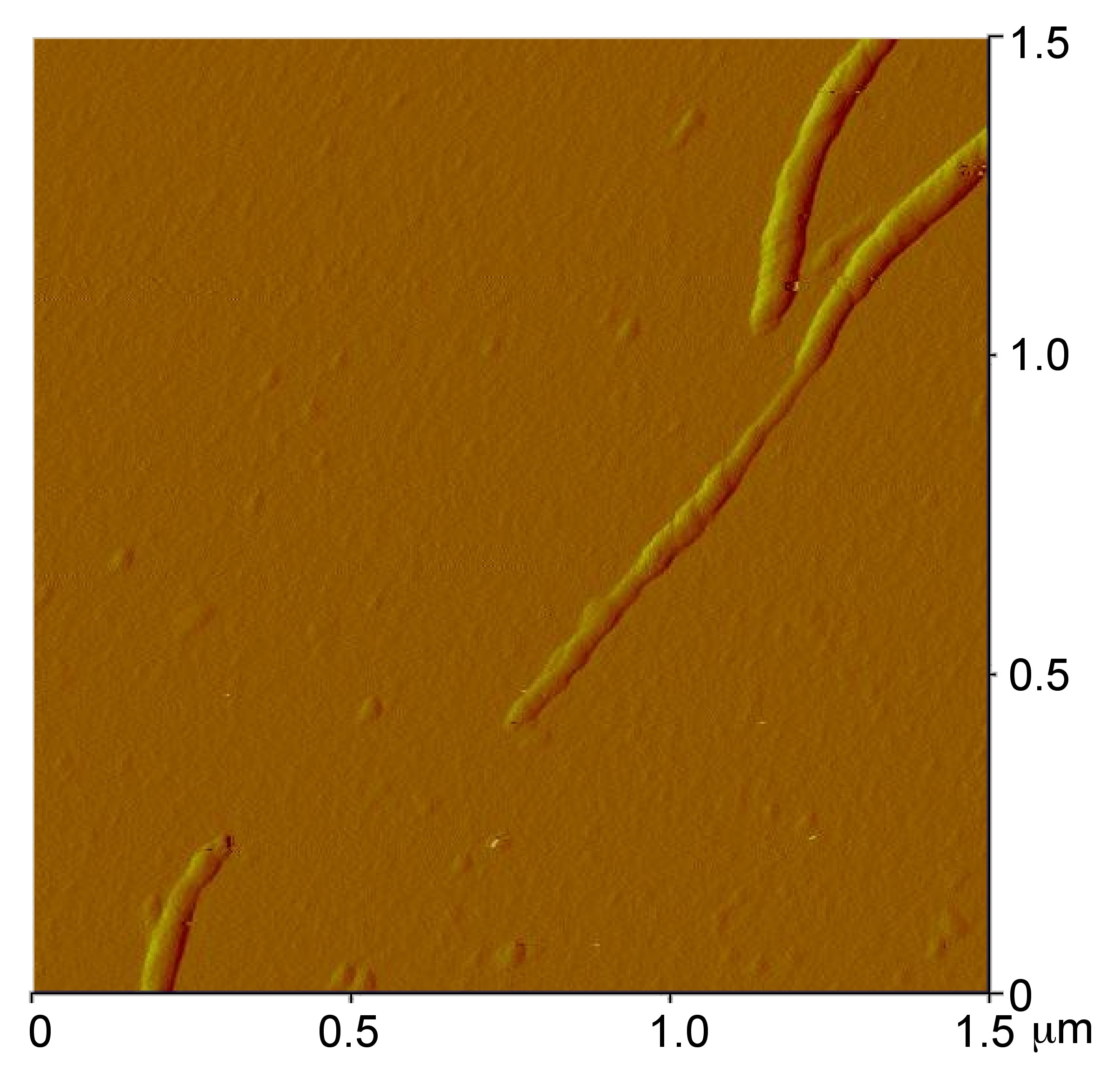
Atomic force microscopy is usually used to study the topographical morphology of these materials. By measuring the thickness of the material it is possible to determine if bundling occurred and to what degree. Other dimensions of the sample can also be measured such as the length and width of the tubes or bundles. It is also possible to detect impurities, functional groups ( [link] ), or remaining catalyst by studying the images. Various methods of producing nanotubes have been found and each demonstrates a slightly different profile of homogeneity and purity. These impurities can be carbon coated metal, amorphous carbon, or other allotropes of carbon such as fullerenes and graphite. These facts can be utilized to compare the purity and homogeneity of the samples made from different processes, as well as monitor these characteristics as different steps or reactions are performed on the material. The distance between the tip and the surface has proven itself to be an important parameter in noncontact mode AFM and has shown that if the tip is moved past the threshold distance, approximately 30 μm, it can move or damage the nanotubes. If this occurs, a useful characterization cannot be performed due to these distortions of the image.

Atomic force microscopy is best applied to aggregates of fullerenes rather than individual ones. While the AFM can accurately perform height analysis of individual fullerene molecules, it has poor lateral resolution and it is difficult to accurately depict the width of an individual molecule. Another common issue that arises with contact AFM and fullerene deposited films is that the tip shifts clusters of fullerenes which can lead to discontinuities in sample images.

Notification Switch
Would you like to follow the 'Chemistry of electronic materials' conversation and receive update notifications?