| << Chapter < Page | Chapter >> Page > |
This slope results due to Base-Width Modulation also known as Early Effect. This we will discuss in the next section.
Next we look at the reverse transmission factor. It is one order of magnitude smaller in CB configuration as compared to that in CE configuration. This means that feed-back from output to input is negligible and BJT is an Unilateral Device in case of CB configuration. Whereas there is much larger feedback from output to input in case of CE configuration and CE BJT behave as an non-Unilateral device. Hence RF Amplifiers which are susceptible to Parasitic Oscillations prefer CB configuration as compared to CE configuration.
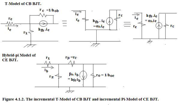
The fact that CB is Unilateral device and CE is non-Unilateral device is evident from Figure 4.1.2. also.

T-Model of CB BJT has two meshes, input mesh and output mesh, which are very weakly interacting through base spreading resistance, r x , and are completely non-interacting if r x = 0. Hence CB BJT is near Unilateral Device and inspecting the diagram we see that:

Hybrid-π Model of CE BJT has two very strongly interacting input and output meshes even if the base spreading resistance is zero. Therefore CE BJT is considered to be non-Unilateral device therefore it is highly susceptible to parasitic oscillations in RF Applications. Hence CE BJT is never utilized for building a RF Amplifier. Inspecting the diagram wew see that:

Input impedance of CB BJT is only 26Ω whereas input impedance of CE BJT is 2.6kΩ at I C = 1mA.
The short circuit current gain in CB BJT is less than Unity hence called short circuit current transfer ratio:

The short circuit current gain in CE BJT is β fo ~ 100. Because of Unity Short Circuit Current Gain in CB BJT, it has a much larger cut-off frequency as compared to that of CE BJT:

Alpha cut-off frequency or Alpha -3dB frequency = 800MHz and
Beta cut-off frequency = 8 MHz.
4.1.1.1. Early Effect or Base-Width Modulation.
As the output voltage in CB or CE configuration varies it leads to variable reverse bias voltage across BC Junction. This leads to variation in the Neutral Base Region. A narrow base gives a better transistor action and a wide base gives a poor transistor action. As output voltage decreases, neutral base width decreases leading to increase in Collector Current. This gives the slope to the output characteristic.
In CB BJT, transistor action is a weak function of W = width of the neutral base hence in CB BJT there is small slope in I-V curve and output impedance is more than 1MΩ at 1mA collector current.
In CE BJT, transistor action is a strong function of W therefore we obtain a larger slope in I-V curve and output impedance falls to 40kΩ at 1mA Collector Current.
Both these points are evident when we look at the output characteristics of CB and CE BJT.
4.1.1.2. Forward Beta (β F ) fall off at low and high currents.
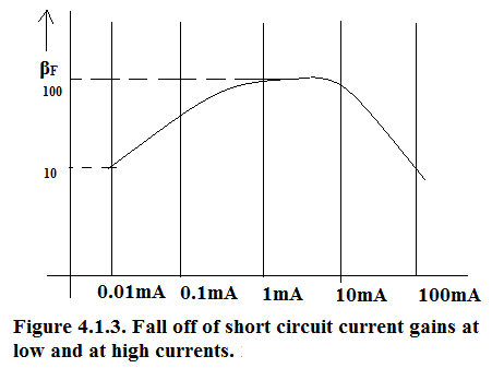
At moderate currents from 0.1mA to 5mA short circuit current gain is constant but it falls off at very low currents and at very high currents as shown in Figure 4.1.3.. Just as in Diode there is a deviation from the ideal Diode equation at low currents due to recombination in the depletion region in exactly the same way the injection efficiency in BJT falls off at low currents due to recombination in the depletion region. This leads to a deterioration in β F at low currents.
Again just as in Diode there is a deviation from ideal Diode equation at high currents due to High Injection Level(HIL) , in the same way there is a conductivity modulation of Base at high currents due to HIL effects. This again leads to the deterioration in injection efficiency and hence in β F at high cureents.
In the design section we will show that for a good injection efficiency conductivity of emitter must be much larger than that of the Base. But this condition is not satisfied at high injection level.


Notification Switch
Would you like to follow the 'Solid state physics and devices-the harbinger of third wave of civilization' conversation and receive update notifications?