| << Chapter < Page | Chapter >> Page > |
AE_Lecture8_PartA Static characteristics of FIELD EFFECT TRANSISTORS
A Field Effect Transistor is like a pentode. It is an analogue of pentode. Both are Voltage Controlled Current Sources.
FET is of two types JFET and MOSFET.
JFET is n channel FET known as nJFET and p channel FET known as pJFET.
Similarly MOS is n channel NMOS and p channel PMOS.
MOS can be enhancement mode which is normally-off or depletion mode normally-on device.
So NMOS can be (E)NMOS and (D)NMOS.
PMOS can be (E)PMOS and (D)PMOS.
The following is the circuit diagram of an Amplifier using N-channel JFET:
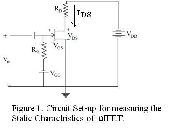
Measurement of characteristics of N-channel JFET
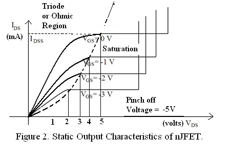
Figure 2 gives the dc output characteristics nJFET. Note that Gate Voltage is always kept negative so that the gate current is always zero. We indicate the Gate-Drain breakdown also. As gate voltage becomes more negative , Avalanche Breakdown of Gate to Drain Junction takes place earlier.When (V DS – V GS ) exceeds V P (Vpinchoff), the channel gets pinched off towards the Drain End and current becomes constant. This is saturation region. The dotted parabola seperates the Ohmic region or Triode Region from Saturation Region or Pentode Region. Here the pinch off voltage is -5V.
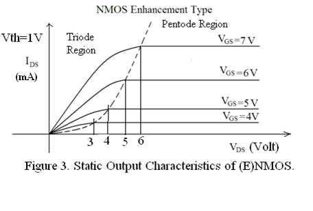
Figure 3 gives the output characteristics of (E)NMOS with a Threshold Voltage of 1V. Therefore when V DS increases and becomes equal to (V GS - V Th ) the channel pinches off near the drain end and current saturates.. As V DS assumes larger values the pinched off region becomes wider, (V GS - V Th ) drops across the channel and excess part of V DS drops across the pinched off region. Since there is a constant voltage dropping across the channel and since the channel is of constant length hence I DS is constant. But in real life there is a shortening of channel length leading to a slope of the saturated current. This channel length modulation is responsible for a finite output impedance r ds of the voltage controlled current source modeling (E)NMOS under incremental condition.
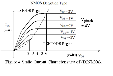
In Figure 4 we give the output characteristics of (D)NMOS. Depletion type device is normally-on device hence it gives a characteristic for positive gate voltage, zero gate voltage and negative voltage. In (D)NMOS when gate voltage becomes equal to Pinch-off voltage then (D)NMOS turns off. Here pinch off voltage is -4V.
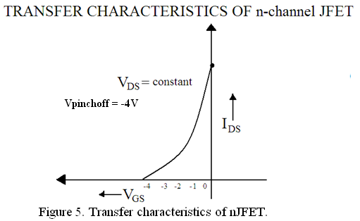
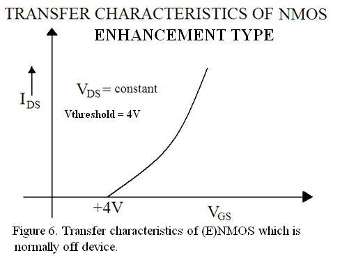
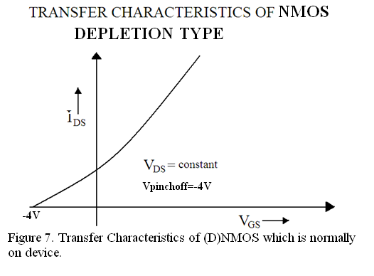
Comparing the transfer characteristics of nJFET, (E)NMOS and (D)NMOS as given in Figure 5, 6 and 7 we can say that (D)NMOS is most flexible device from design point of view as it accepts both positive and negative voltages as the gate voltage.
NMOS Transistor (Pentode and Triode Region)
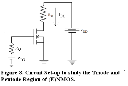
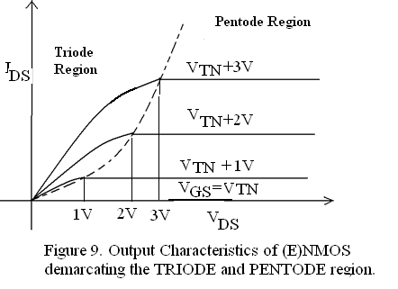
TRIODE REGION:

K
n =
K
n
' multiplied_by

K n '= µ n C ox ″ ...........Kn’ ia a transconductance parameter which is fixed for a given technology and cannot be changed by the circuit designer.Whereas Kn = Kn’×(W/L) = this is also a transconductance parameter but it includes the aspect ration (W/L) of the given MOSFET. The aspect ratio gives the geometry of the device and this is under control of a circuit designer . This second transconductance parameter can be controlled when he is generating the masks for a given circuit or system during ASIC(Application Specefic IC) or SOC(System –on- Chip) design. W is the width of the gate andL is the length of the gate or the length of the channel.


Triode Region exists as long as

Channel should not pinch off on the drain side.
PENTODE REGION
At

channel pinches off at drain end. From here onwards current becomes constant or current saturates.
Substituting (2) in (1),


Where:


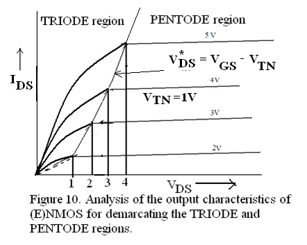
Pinch Off locus is parabolic

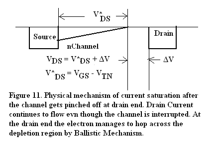
For any V GS , at V* DS = V GS - V TN the saturation sets in as the channel gets pinched off at that point. Beyond that point: V DS = V* DS + ΔV and V* DS drops across the channel and ΔV drops across the depleted region towards the drain end as shown in Figure 11. Since the voltage across the channel is constant at V* DS and since the channel is approximately constant ( it shortens slightly as Drain to Source Voltage increases) for practical purposes we assume that the drain current is constant and hence it has saturated. But in practice due to channel length shortening, there is slight increase in drain current with drain to source voltage. Hence output characteristics does have a slope. At higher currents the slope is higher.
K n =25 µA/V 2

N channel JET has identical formulation except threshold voltage is replaced by pinch off voltage.

Notification Switch
Would you like to follow the 'Solid state physics and devices-the harbinger of third wave of civilization' conversation and receive update notifications?