| << Chapter < Page | Chapter >> Page > |
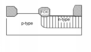
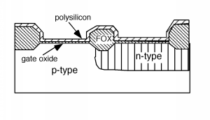
Then the gate oxide is grown, and immediately thereafter, the whole wafer is covered with polysilicon [link] .
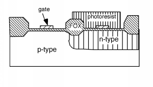
The polysilicon is then patterned to form the two regions which will be our gates. The wafer is covered once again withphotoresist. The resist is removed over the region that will be the n-channel device, but is left covering the p-channeldevice. A little area near the edge of the n-tank is also uncovered [link] . This will allow us to add some additional phosphorus into the n-well, so that we can make acontact there, so that the n-well can be connected to .
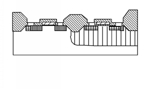
Back into the implanter we go, this time exposing the wafer to phosphorus. The poly gate, the FOX and the photoresist all blockphosphorus from getting into the wafer, so we make two n-type regions in the p-type substrate, and we have made our n-channelMOS source/drain regions. We also add phosphorous to the contact region in the n-well so as the make sure we get good contact performance there [link] .
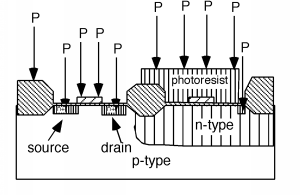
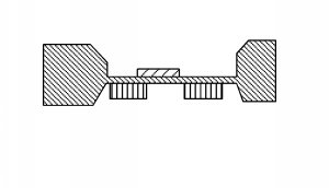
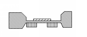
The formation of the source and drain were performed with a self-aligning technology . This means that we used the gate structure itself to define where the two insideedges of the source and drain would be for the MOSFET. If we had made the source/drain regions before wedefined the gate, and then tried to line the gate up right over the space between them, we might have gotten something thatlooks like what is shown in [link] . What's going to be the problem with this transistor? Obviously, if thegate does not extend all the way to both the source and the drain, then the channel will noteither, and the transistor will never turn on! We could try making the gate wider, to ensure that it will overlap bothactive areas, even if it is slightly misaligned, but then you get a lot of extraneous fringing capacitance which willsignificantly slow down the speed of operation of the transistor [link] . This is bad! The development of the self-aligned gate technique was one of the big breakthroughswhich has propelled us into the VLSI and ULSI era.
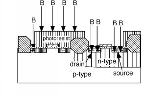
We pull the wafer out of the implanter, and strip off the photoresist. This is sometimes difficult, because the act of ionimplantation can "bake" the photoresist into a very tough film. Sometimes an rf discharge in an O 2 atmosphere is used to "ash" the photoresist, and literally burnit off the wafer! We now apply some more PR, and this time pattern to have the moat area, and a substrate contact exposed,for a boron p + implant. This is shown in [link] .
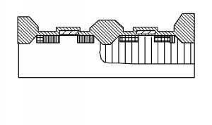
We are almost done. The next thing we do is remove all the photoresist, and grow one more layer of oxide, which coverseverything, as shown in [link] . We put photoresist over the whole wafer again, and pattern for contactholes to go through the oxide. We will put contacts for the two drains, and for each of the sources, make sure that the holesare big enough to also allow us to connect the source contact to either the p-substrate or the n-moat as is appropriate [link] .

Notification Switch
Would you like to follow the 'Chemistry of electronic materials' conversation and receive update notifications?