| << Chapter < Page | Chapter >> Page > |
Advent of multi-touch intuitive interface and its dependent application has increaded the expectations from the User Interface. Today following are our expectations from our User Interface namely:
These User Interface capabilities are already available in health monitoring, exercise and environmental control tools. These capabilities are also coming on wrist watches, smart clothing and smart shoes. In order that these subtle capabilities are realized we need smart phones to be “instantly on, always on, always connected and always aware.” This will enable:
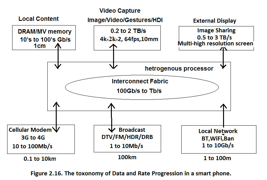
The advent of ultra low power wireless sensor nodes in the immediate environment of smart phones will provide valuable local information that requires constant awareness from the smart phone. Smart phones will need to interact with resources in the environment- this will require high data rate links with high energy efficiency of transmission. The huge increase in data communication requires significant reduction in the amount of energy spent per bit when transmitting all the data.

The moble revolution has been enabled by Silicon Technology Scaling but this is not adequate to meet the exponentially increasing needs of computation. We need 100 times greater enery efficieny to meet the exploding computational needs. To this end we need the following:
“Collectively the resulting advances will provide wealth of information to the key-hub and the ultimate link to the cloud – the smart phone – catapulting us into an exciting new technological world.”
2.1.2.6. CMOS Technology is the technology of choice for all applications as we make a transition from micro to nano era.
[“The Age of Digital Nomad- Impact of CMOS innovation’, Tsugio Makimeto, IEEE Solid State Circuits Magazine, Winter 2013, Vol.5, No.1]
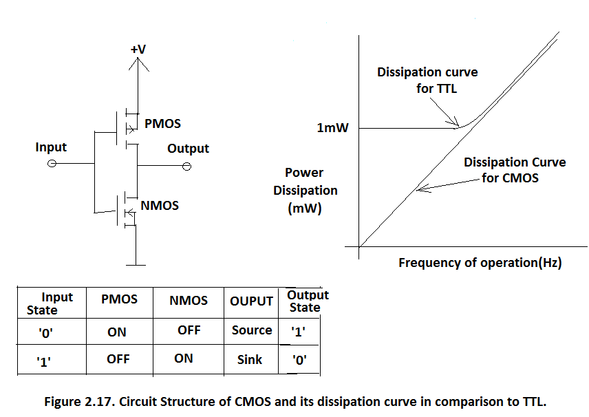
A CMOS inverter is a nano-watt logic because its stand-by power dissipation is in nano-watt. Hence right from the beginning it has been the Technology of Choice in microprocessor design and fabrication. Its circuit configuration and its power dissipation curve are shown in Figure 2.17.

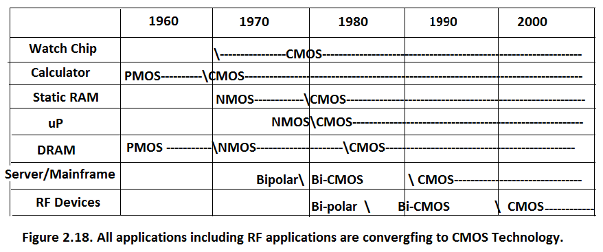
As we move from Micron Technology (Channel length is greater than 1μm) to sub-micron Technology(Channel length is between 990nm-100nm) to deep-submicron Technology(Channel length is between 100nm-50nm) to ultra-deep-submicron Technology(Channel length is between 50nm-10nm), power management and power dissipation are becoming bigger and more crucial issue hence all applications are converging to CMOS technology because of its zero stand-by feature as seen in Figure 2.18.
There was clear demarcation among consumer, computer and communication systems but with the advances of Semiconductor Technology they are collectively called digital consumer products. This market convergence and this market convergence is being driven by digitization of information and CMOS innovation.

Today the hall mark of Solid State Systems are still more clearly defined and are visible:
Figure of Merit=Intelligence/(Size*Cost*Power). Here intelligence is defined as MIPS(Mega Instruction per second) for general purpose computers; MOPS(Mega Operations per second) for signal processor and FLOPS(Floating Point Operations per second) for numerical calculating systems.
Semiconductor Technology has made great progress towards maximizing the Figure of Merit.

Notification Switch
Would you like to follow the 'Solid state physics and devices-the harbinger of third wave of civilization' conversation and receive update notifications?