<< Chapter < Page Chapter >> Page >
This module was developed as part of the Rice University course CHEM-496: Chemistry of Electronic Materials . This module was prepared with the assistance of Zane Ball.

Introduction

Photolithography is one of the most important technology in the production of advanced integrated circuits. It is through photolithography that semiconductor surfaces are patterned and the circuits formed. In order to make extremely small features, on the order of the wavelength of the light, advanced optical techniques are used to transfer a pattern from a mask onto the surface. A polymeric film or resist , is modified by the light and records the information in a process not dissimilar to ordinary photography.

An illustration of the photolithographic process is shown in [link] . The process follows the following basic steps:
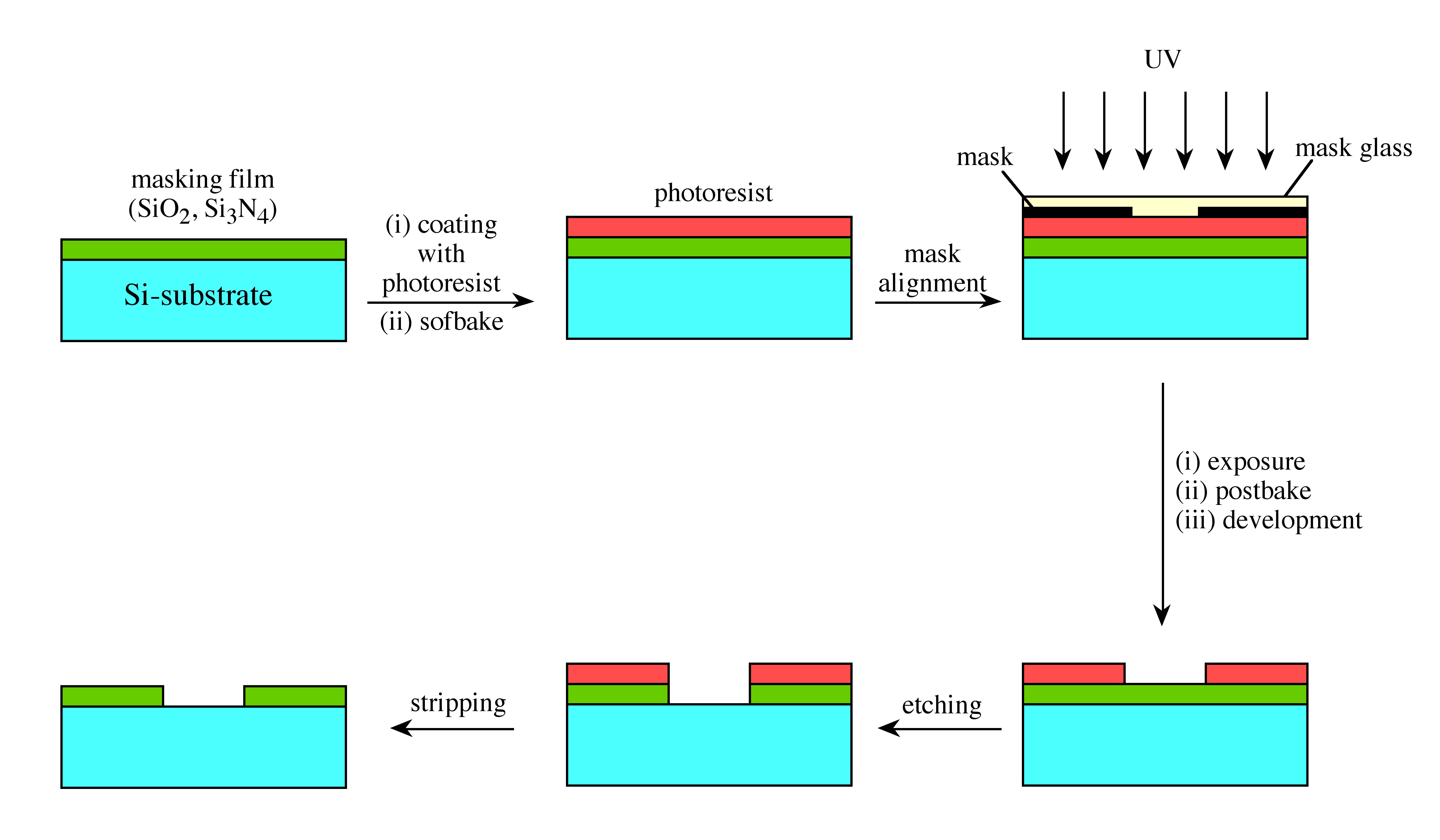
  1. The wafer is spin coated with resist to form a uniform ~1 µm thin film of resist on the surface.
  2. The wafer is exposed with ultraviolet light through a mask which contains the desired pattern. In the simplest processes the mask is simply placed over the wafer, but advanced sub-micron technologies require the pattern to imaged through a complex optical system.
  3. The photoresist is developed and the irradiated area is washed away (positive resist) or the unirradiated area is washed away (negative resist).
  4. Processing (etching, deposition etc.)
  5. Remaining resist is stripped.
Steps in optical printing using photolithography.

In addition to being possibly the most important semiconductor process step, photolithography is also the most expensive technology in semiconductor manufacturing. This expense is the result of two considerations:

  1. The optics in photolithography tools are expensive where a single lens can cost a $1 million or more
  2. Each chip (often referred to as a "dye") must be exposed individually unlike other semiconductor processes such as CVD where an entire wafer can be processed at a time or oxidation processes where many wafers can be processed simultaneously.

This means that not only are photolithography machines the most expensive of semiconductor processing equipment, but more of them are needed in order to maintain throughput.

Optical issues in photolithography

The critical dimension and depth of focus

A semiconductor process technology is often described by a characteristic length known as the critical dimension. The critical dimension (CD) is the smallest feature that needs to be patterned on the surface. The exact definition varies from process to process but is often the channel length of the smallest transistor (typical of a memory chip) or the width of the smallest metal interconnection line (logic chips). This critical dimension is defined by the photolithographic process and is perhaps the most important figure of merit in the manufacture of integrated circuits. Making the critical dimension smaller is the primary focus of improving semiconductor technology for the following reasons:

  1. Making the CD smaller dramatically increases the number of devices per unit area and this increase goes with the square of the CD (i.e., a reduction in CD by a factor of 2 generates 4 times the number of devices).
  2. Making the CD smaller of a device already in production will make a smaller chip. This means that the number of chips per wafer increases dramatically, and since costs generally scale with the number of wafers and not the number of chips to a wafer, costs are dramatically reduced.
  3. Smaller devices are faster.

Questions & Answers

A golfer on a fairway is 70 m away from the green, which sits below the level of the fairway by 20 m. If the golfer hits the ball at an angle of 40° with an initial speed of 20 m/s, how close to the green does she come?
Aislinn Reply
cm
tijani
what is titration
John Reply
what is physics
Siyaka Reply
A mouse of mass 200 g falls 100 m down a vertical mine shaft and lands at the bottom with a speed of 8.0 m/s. During its fall, how much work is done on the mouse by air resistance
Jude Reply
Can you compute that for me. Ty
Jude
what is the dimension formula of energy?
David Reply
what is viscosity?
David
what is inorganic
emma Reply
what is chemistry
Youesf Reply
what is inorganic
emma
Chemistry is a branch of science that deals with the study of matter,it composition,it structure and the changes it undergoes
Adjei
please, I'm a physics student and I need help in physics
Adjanou
chemistry could also be understood like the sexual attraction/repulsion of the male and female elements. the reaction varies depending on the energy differences of each given gender. + masculine -female.
Pedro
A ball is thrown straight up.it passes a 2.0m high window 7.50 m off the ground on it path up and takes 1.30 s to go past the window.what was the ball initial velocity
Krampah Reply
2. A sled plus passenger with total mass 50 kg is pulled 20 m across the snow (0.20) at constant velocity by a force directed 25° above the horizontal. Calculate (a) the work of the applied force, (b) the work of friction, and (c) the total work.
Sahid Reply
you have been hired as an espert witness in a court case involving an automobile accident. the accident involved car A of mass 1500kg which crashed into stationary car B of mass 1100kg. the driver of car A applied his brakes 15 m before he skidded and crashed into car B. after the collision, car A s
Samuel Reply
can someone explain to me, an ignorant high school student, why the trend of the graph doesn't follow the fact that the higher frequency a sound wave is, the more power it is, hence, making me think the phons output would follow this general trend?
Joseph Reply
Nevermind i just realied that the graph is the phons output for a person with normal hearing and not just the phons output of the sound waves power, I should read the entire thing next time
Joseph
Follow up question, does anyone know where I can find a graph that accuretly depicts the actual relative "power" output of sound over its frequency instead of just humans hearing
Joseph
"Generation of electrical energy from sound energy | IEEE Conference Publication | IEEE Xplore" ***ieeexplore.ieee.org/document/7150687?reload=true
Ryan
what's motion
Maurice Reply
what are the types of wave
Maurice
answer
Magreth
progressive wave
Magreth
hello friend how are you
Muhammad Reply
fine, how about you?
Mohammed
hi
Mujahid
A string is 3.00 m long with a mass of 5.00 g. The string is held taut with a tension of 500.00 N applied to the string. A pulse is sent down the string. How long does it take the pulse to travel the 3.00 m of the string?
yasuo Reply
Who can show me the full solution in this problem?
Reofrir Reply
Got questions? Join the online conversation and get instant answers!
Jobilize.com Reply

Get Jobilize Job Search Mobile App in your pocket Now!

Get it on Google Play Download on the App Store Now


Source:  OpenStax, Chemistry of electronic materials. OpenStax CNX. Aug 09, 2011 Download for free at http://cnx.org/content/col10719/1.9
Google Play and the Google Play logo are trademarks of Google Inc.

Notification Switch

Would you like to follow the 'Chemistry of electronic materials' conversation and receive update notifications?

Ask