| << Chapter < Page | Chapter >> Page > |
Tutorial Sheet of Chapter 2.Semiconductor Physics.
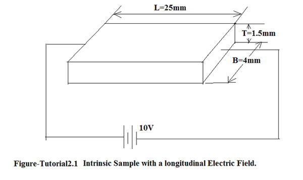
Question 1. (a)Determine the Drift Velocity of electron and hole in the given intrinsic sample in Figure-Tutorial 2.1. with 10V applied across the junction?[vdrift(n)=5800cm/s,vdrift(p)=1800cm/s]Assume mobility given for intrinsic sample.
(b)Determine the conductivity of the following intrinsic sample?[σ=3*10 -6 S/cm]
(b) Determine the current flowing though the intrinsic sample?[0.72microA]

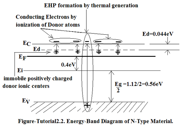
Question 2. The energy-band diagram is given in Figure-Tutorial2.2.

Question 3 .In a P-Type material, E F -E V = 0.1 eV and E a -E V =0.045eV.
Calculate the % of ionization of Acceptor Atoms ? [89%]
Question 4 .There is a compensated P-Type material at 300K. Minority carrier concentration is measured to be n p - =10 6 /cc. Acceptor Dopent Concentration = 10 15 /cc.
Question 5. In Copper, resistivity= ρ = 1.67×10 -8 Ω-m and conductivity = σ = 6×10 7 S/m=qμn and n=8.5×10 22 /m 3 . Determine electron mobility ? [40 cm 2 /(V-s) ]
Question 6. In a 3 m long Cu Wire R = 0.03Ω and I = 15A through the wire.
Question 7. Typical N-Type resistivity ρ S =1Ω-cm.Typical current density 100A/cm 2 . mobility of electrons=1000cm 2 /V-s
Question 8 .In a P-Type Sample , E=10 3 V/cm is applied. Determine drift velocity, mean free time and mean free path ? Assume μ p = 470 cm 2 /(V-s).
[Drift velocity = 4.7×10 5 cm/s which is much lower than thermal velocity of holes=2.2×10 7 cm/s; τ = 0.1ps, Mean Free Path = 220A°]
Question 9. The effective mass of electron and hole in semi-conductor is different from the mass in free space . Why?
The electrons and holes in a crystal interact with the periodic Coulombic Field in the Crystal. They surf over the periodic potential variation of the crystal lattice in the process developing roller coaster effect which leads to drastic reduction in effective mass.
| Si | Ge | GaAs | InAs | AlAs | |
|---|---|---|---|---|---|
| m n /m 0 | 0.26 | 0.12 | 0.068 | 0.023 | 2.0 |
| m p /m 0 | 0.39 | 0.30 | 0.50 | 0.30 | 0.3 |
m n /m 0 = effective mass of electron/free space mass of electron
m p /m 0 = effective mass of hole/free space mass of hole.
In Silicon, using the effective mass of electron and holes the thermal velocity = 2.5×10 7 cm/s. Scatter Limit Velocities of electron and hole are of the same order.

Notification Switch
Would you like to follow the 'Solid state physics and devices-the harbinger of third wave of civilization' conversation and receive update notifications?