| << Chapter < Page | Chapter >> Page > |
Crystal Growth- Bulk and Epitaxial Film- Part2.
SLICING OF SINGLE CRYSTAL INGOT INTO SILICON WAFERS
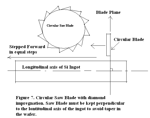
Slicing of the Si ingot into Si wafers is achieved by circular saw blade. The circular saw blade is illustrated in Figure 7.

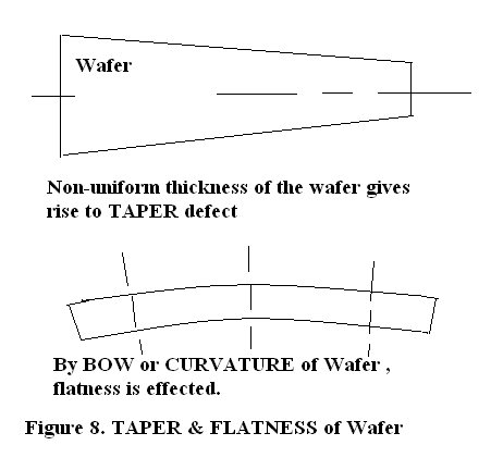
Circular saw blade consists of stainless steel impregnated with diamond dust at the cutting edge. On the hardness scale diamond is the hardest. 500 micrometres thick Si wafers are sliced out through damage free and parallel sawing. The ingot should be sawed in parallel planes to avoid taper of the wafer.

In the process of sawing , mechanical, defects are inevitable. To remove the mechanical defects and to achieve taper-free, flat, mirror finish wafers we do lapping, chemical etching and polishing.
LAPPING : For removing mechanical scratches and abrasions encountered during sawing, lapping is essential. A batch of wafers are placed between two parallel plain steel discs which describe planetry motion in relation to each other. A slurry of cutting compound (generally alumina) is used and as lapping progresses, the grade of abrasion is refined. Smoothness is within 10 μm and flatness is within 2 μm.
CHEMICAL ETICHING : To remove edge damages which had been caused due to sawing and grinding, the wafers is dipped in HF acid using Teflon beakers. Chemical Vapor etching can also be done as described in epitaxy section.
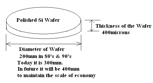
POLISHING : A slurry of silica in NaOH is used for polishing to mirror smoothness. Lapping , Chemical Etching and Polishing removes 100μm thick substrate leaving behind 400μm thick silicon substrate on which I.C. Fabrication can be carried out..
FLOW CHART OF WAFER PREPARATION
Starting Material - Sand, Sand reduced to Silicon, Silicon converted to TriChloroSilane, through multiple distillation TrichloroSilane is purified to Electronic Grade and reduced in Siemen’s Reactor to Pure Electronic Grade Polycrystalline Si.
↓
From purified Silicon Melt, single crystal ingot is pulled out by Czochralski Method or Poly Si ingot is purified re- crystallized by Float Zone Method. Required Dopent ( Phosphoprous for N Type ingot and Boron for P Type ingot) is added to the melt in calculated manner to form single crystal ingot of specific impurity type doping and of given resistivity.
↓
Sawing, Lapping, Grinding and Polishing
↓

In early days when IC Technology had just started i.e. in the year 1961 the wafer size was only 1 inch. Then it was:* 2 inch (50.8 mm). Thickness 275 µm. * 3 inch (76.2 mm). Thickness 375 µm.* 4 inch (100 mm). Thickness 525 µm. * 5 inch (127 mm) or 125 mm (4.9 inch). Thickness 625 µm.* 150 mm (5.9 inch, usually referred to as "6 inch"). Thickness 675 µm. * 200 mm (7.9 inch, usually referred to as "8 inch"). Thickness 725 µm.* 300 mm (11.8 inch, usually referred to as "12 inch" or "Pizza size" wafer). Thickness 775 µm. * 450 mm ("18 inch"). Thickness 925 µm (expected).By all these technique , high purity (99.999%) single crystal ingots with a controlled amount of N or P type dopent can be produced. The maximum resistivity obtained in Si ingot is 10 4 Ω-cm whereas in Ga As and InP the ρmax =10 8 Ω-cm. That is almost semi-insulating ingot of GaAs and InP can be obtained. Semi-insulating GaAS and InP wafers are suitable for reduction of parasitics, for isolaton of active devices from one another, for reduction of power drain and for achieving high speed.
Presently because of technical constraints we have the option of Si, GaAs and InP substrate only. Therefore we have a very limited choice of overlay films also. This severely constrains the photonic device design.

Notification Switch
Would you like to follow the 'Solid state physics and devices-the harbinger of third wave of civilization' conversation and receive update notifications?