| << Chapter < Page | Chapter >> Page > |
Following this, the control unit sends a control signal that opens gates between the MBR and the IR.
This completes the fetch cycle except for one thing: The control unit must decide whether to perform an indirect cycle or an execute cycle next. To decide this, it examines the IR to see if an indirect memory reference is made.
The indirect and interrupt cycles work similarly. For the execute cycle, the control unit begins by examining the opcode and. on the basis of that, decides which sequence of micro-operations to perform for the execute cycle.
A Control Signals Example
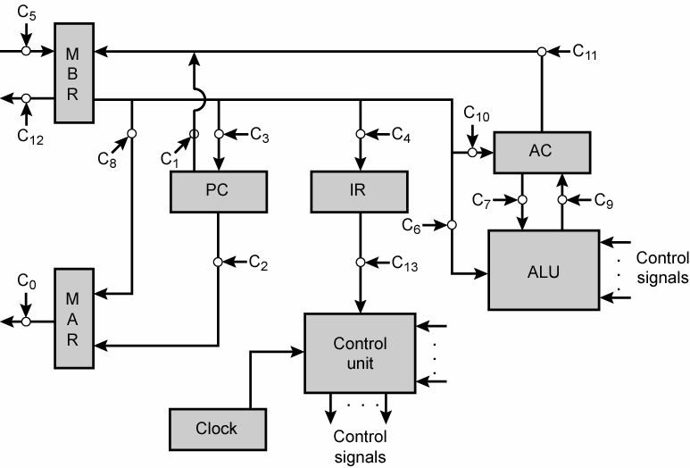
To illustrate the functioning of the control unit, let us examine a simple example. Figure 6.5 illustrates the example.

Figure 6.5 Data Paths and Control Signals
This is a simple processor with a single accumulator. The data paths between elements are indicated. The control paths for signals emanating from the control unit are not shown, but the terminations of control signals are labeled Ci and indicated by a circle. The control unit receives inputs from the clock, the instruction register, and flags. With each clock cycle, the control unit reads all of its inputs and emits a set of control signals. Control signals go to three separate destinations:
The control unit must maintain knowledge of where it is in the instruction cycle. Using this knowledge, and by reading all of its inputs, the control unit emits a sequence of control signals that causes micro-operations to occur.
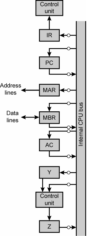
Figure 6.5 indicates the use of a variety of data paths. The complexity of this type of organization should be clear. More typically, some sort of internal bus arrangement. Using an internal processor bus, Figure 6.5 can be rearranged as shown in Figure 6.6.

Figure 6.6 CPU with Internal Bus
A single internal bus connects the ALU and all processor registers. Gates and control signals are provided for movement of data onto and off the bus from each register. Additional control signals control data transfer to and from the system (external) bus and the operation of the ALU.
Two new registers, labeled Y and Z have been added to the organization. These are needed for the proper operation of the ALU. When an operation involving two operands is performed, one can be obtained from the internal bus, but the other must be obtained from another source. The AC could be used for this purpose, but this limits the flexibility of the system and would not work with a processor with multiple general-purpose registers. Register Y provides temporary storage for the other input. The ALU is a combinatorial circuit with no internal storage, Thus, when control signals activate an ALU function, the input to the ALU is transformed to the output. Thus, the output of the ALU cannot be directly connected to the bus, because this output would feed back to the input. Register Z provides temporary output storage, with this arrangement, an operation to add a value from memory to the AC would have the following steps:
t1: MAR<= (IR(address))
t2: MBR<= Memory
t3: Y<= (MBR)
t4: Z<= (AC0 + (Y)
t5: ac<= (z)
Other organizations are possible, but, in general, some sort of internal bus or set of internal buses is used. The use of common data paths simplifies the interconnection layout and the control of the processor. Another practical reason for the use of an internal bus is to save space. Especially for microprocessors, which may occupy only a 1/4-inch square piece of silicon, space occupied by internal connections must be minimized.

Notification Switch
Would you like to follow the 'Computer architecture' conversation and receive update notifications?