| << Chapter < Page | Chapter >> Page > |
1. Semiconductor Main Memory
The basic element of a semiconductor memory is the memory cell. There are a lot of semiconductor memory types shown in table 11.1
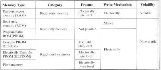
Table 11.1 Semiconductor Memory Types
RAM: Read-write memory
The two basic forms of semiconductor Random Access Memory (RAM) are dynamic RAM (DRAM) and static RAM (SRAM). SRAM is faster, more expensive and less dense than DRAM. DRAM is usually used for main memory.
- Storage cell is essentially a transistor acting as a capacitor
- Capacitor charge dissipates over time causing a 1 to flip to a zero
- Cells must be refreshed periodically to avoid this
- Very high packaging density
- Uses 5-10x more transistors than similar dynamic cell so packaging density is 10x lower
- Faster than a dynamic cell
ROM : Read Only Memories
A Read only Memory (ROM) contain a permanent of data that canot be changed.
- “Permanent” data storage
- ROMs: Data is “wired in” during fabrication at a chip manufacturer’s plant
- Purchased in lots of 10k or more
- Data can be written once by the user employing a PROM programmer
- Useful for small production runs
- Programming is similar to a PROM
- Can be erased by exposing to UV light
- Can be written to many times while remaining in a system
- Does not have to be erased first
- Program individual bytes
- Writes require several hundred usec per byte
- Used in systems for development, personalization, and other tasks requiring unique information to be stored
- Fast erasures, block erasures
- Higher density than EEPROM
Each memory chip contains a number of 1-bit cells. The 1, 4, and 16 million cell chips are common. The cells can be arranged as a single bit column (e.g., 4Mx1) or in multiple bits per address location (e.g., 1Mx4)
- To reduce pin count, address lines can be multiplexed with data and/or as high and low halves Trade off is in slower operation
W* (write), OE* (output enable) for write and read operations
CS* (chip select) derived from external address decoding logic
RAS*, CAS* (row and column address selects) used when address is applied to the chip in 2 halves
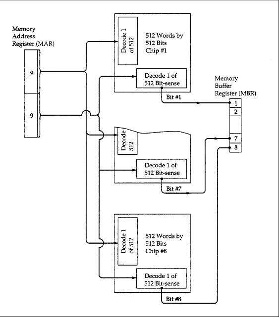
Figure 11.1 Organization 256Kx8 memory from 256Kx1 chips
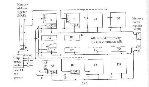
Figure 11.2 . Mbyte Memory Organization
– Hard (permanent) errors
» Environmental abuse
» Manufacturing defects
» Wear
– Soft (transient) errors
» Power supply problems
» Alpha particles: Problematic as feature sizes shrink
– Memory systems include logic to detect and/or correct errors
» Width of memory word is increased
» Additional bits are parity bits
» Number of parity bits required depends on the level of detection and correction needed
– A single error is a bit flip -- multiple bit flips can occur in a word
– 2M valid data words
– 2M+K codeword combinations in the memory
– Distribute the 2M valid data words among the 2 M+K codeword combinations such that the “distance” between valid words is sufficient to distinguish the error
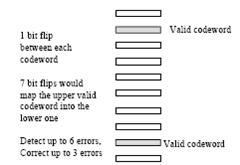
Figure 11.3
– For each valid codeword, there will be 2K-1 invalid codewords
– 2K-1 must be large enough to identify which of the M+K bit positions is in error
– Therefore 2K-1>M+K
» 8-bit data, 4 check bits
» 32-bit data, 6 check bits
– Arrange bits as shown in Figure 11.4
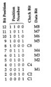
Figure 11.4
– Bit position n is checked by bits Ci such that the sum of the subscripts, i, equals n (e.g., position 10, bit M6, is checked by bits C2 and C8)
To detect errors, compare the check bits read from memory to those computed during the read operation (use XOR)
+ If the result of the XOR is 0000, no error
+ If non-zero, the numerical value of the result indicates the bit position in error
+ If the XOR result was 0110, bit position 6 (M3) is in error
Double error detection can be added by adding another check bit that implements a parity check for the whole word of M+K bits. SED and SEC-DED are generally enough protection in typical systems

Notification Switch
Would you like to follow the 'Computer architecture' conversation and receive update notifications?