| << Chapter < Page | Chapter >> Page > |
The Journey of I.C.Technology from micro (1959) to nano (2009) era.-Part 7.
Keywords: Sidewall Oxidation Technique, Trench Isolation Technique, Reactive Ion Etching.
Summary: This Part 7 of 50 years journey;
IV.1.5. Sidewall oxidation and Silicon-on-Insulator for reducing the parasitic capacitances and improving the frequency response.
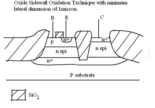
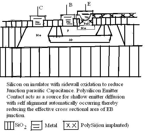
Large junction parasitic capacitances are introduced due to Silicon P-type substrate and due to sidewalls of isolation diffusion. Substrate capacitances can be eliminated by using Silicon-on Sapphire or by Silicon-on-Insulator. Isolation diffusion side-wall junction can be eliminated by using sidewall oxidation.
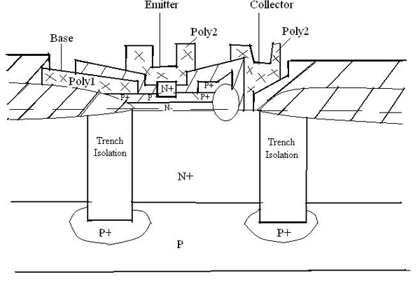
These structures are shown in Figure 7 and Figure 8. P+ isolation diffusion can be replaced by Trench isolation by Reactive Ions Etching (RIE) as shown in Figure 9.

Figure 9. Oxide Sidewall Oxidation Technique to minimize the parasitic capacitances.

Figure 10. Cross sectional view of an advanced self aligned polysilicon Emitter BJT with side wall oxidation and Silicon on Insulator for reducing the parasitic capacitances.

Figure 11.Cross-Section diagram of an advanced double self-aligned polysilicon emitter BJT with sidewall oxide and trench isolation.
[10.7GHz BJT using double layer process technology, Electroniuc Letters Vol.24,920-22, July 1988]
P + isolation diffusion is replaced by trench isolation. Trench Isolation is achieved by Reactive Ion Etching(RIE). Emitter and Base regions are self aligned to minimize A E . Oxide side wall used for reducing junction capacitance.

Notification Switch
Would you like to follow the 'Solid state physics and devices-the harbinger of third wave of civilization' conversation and receive update notifications?