| << Chapter < Page | Chapter >> Page > |
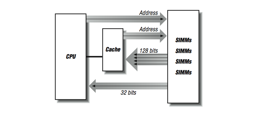
A further advantage of bypassing cache is that the data doesn’t need to be moved through the SRAM cache. This operation can add from 10–50 ns to the load time for a single word. This also avoids invalidating the contents of an entire cache line in the cache.
Adding cache bypass, increasing memory-system widths, and adding banks increases the cost of a memory system. Computer-system vendors make an economic choice as to how many of these techniques they need to apply to get sufficient performance for their particular processor and system. Hence, as processor speed increases, vendors must add more of these memory system features to their commodity systems to maintain a balance between processor and memory-system speed.
Bypassing cache

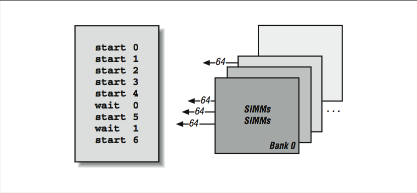
Vector supercomputers, such as the CRAY Y/MP and the Convex C3, are machines that depend on multibanked memory systems for performance. The C3, in particular, has a memory system with up to 256-way interleaving. Each interleave (or bank) is 64 bits wide. This is an expensive memory system to build, but it has some very nice performance characteristics. Having a large number of banks helps to reduce the chances of repeated access to the same memory bank. If you do hit the same bank twice in a row, however, the penalty is a delay of nearly 300 ns — a long time for a machine with a clock speed of 16 ns. So when things go well, they go very well.
However, having a large number of banks alone is not sufficient to feed a 16-ns processor using 50 ns DRAM. In addition to interleaving, the memory subsystem also needs to be pipelined. That is, the CPU must begin the second, third, and fourth load before the CPU has received the results of the first load as shown in [link] . Then each time it receives the results from bank “n,” it must start the load from bank “n+4” to keep the pipeline fed. This way, after a brief startup delay, loads complete every 16 ns and so the memory system appears to operate at the clock rate of the CPU. This pipelined memory approach is facilitated by the 128-element vector registers in the C3 processor.
Using gather/scatter hardware, non-unit-stride operations can also be pipelined. The only difference for non-unit-stride operations is that the banks are not accessed in sequential order. With a random pattern of memory references, it’s possible to reaccess a memory bank before it has completely refreshed from a previous access. This is called a bank stall .
Multibanked memory system

Different access patterns are subject to bank stalls of varying severity. For instance, accesses to every fourth word in an eight-bank memory system would also be subject to bank stalls, though the recovery would occur sooner. References to every second word might not experience bank stalls at all; each bank may have recovered by the time its next reference comes around; it depends on the relative speeds of the processor and memory system. Irregular access patterns are sure to encounter some bank stalls.

Notification Switch
Would you like to follow the 'High performance computing' conversation and receive update notifications?