| << Chapter < Page | Chapter >> Page > |
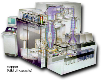
Next, a machine called a stepper ( [link] ) is calibrated to project an extremely fine and focused image through a special type ofreticle film in a manner similar to that of a simple slide projector. The light that is transmitted through the reticle isprojected onto the photoresist layer, which reacts to the light and begins to harden. All of the parts of the wafer exposed to thislight harden into a tough crust while the parts in shadow remain soft. This particular step is known by the name ofphotoelectrochemical etching because it achieves an etching effect, resulting in a chip.

Hundreds of copies of the chip are etched onto the wafer until the entire surface has been exposed. Once this process is complete, the entirewafer is submerged into an etching bath, which washes away any parts of the photoresist that remain unexposed along with theinsulating chemicals underneath. The hardened areas of the photoresist, however, remain and protect the layers of materialunderneath them. This process of depositing chemicals, coating with a photoresist, exposure to light over a film mask, and etching andwashing away is repeated more than a dozen times. The result is an elaborate, three-dimensional construction of interlocking siliconwires.
This product is then coated with another insulating layer and is plated with a thin layer of metal, usuallyeither aluminum or copper. Yet another photoresist is laid down on top of this metal plating, and after the wafer is exposed in astepper, the process repeats with another layer of metal. After this step has been repeated several more times, a final wash stepis performed, and a finished semiconductor product rolls off the assembly line, at last.
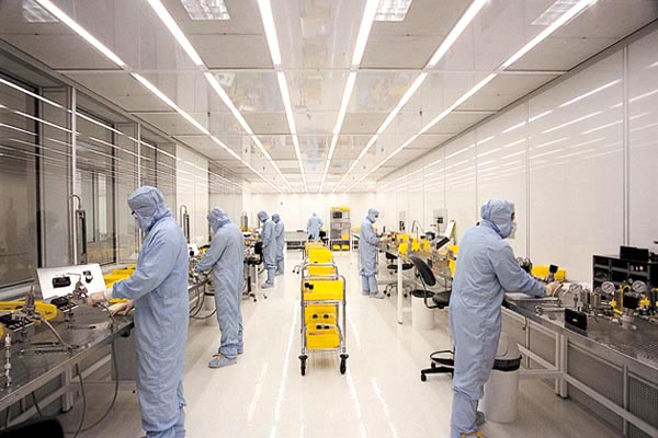
A typical semiconductor fabrication facility, or “fab” in industry jargon, looks like a normal two- or three-story officebuilding from the outside, and most of the interior space is devoted to one or more “clean rooms,” in which the semiconductorsare actually made. A clean room is designed with a fanatical attention to detail aimed towards keeping the room immaculate anddust-free ( [link] ).

Most if not all surfaces inside these clean rooms are composed of stainless steel, and these surfaces aresloped whenever possible or perforated by grating to avoid giving dust a place to settle. The air is filtered through both theceiling and the floor to remove particles that are down to 1/100 the width of a human hair. Lighting is characteristically brightand slightly yellowish to prevent mildew from forming behind equipment or in recessed corners, and even the workers in a cleanroom must be absolutely spotless.
Workers in these rooms must be covered from head to toe in “bunny suits” that completely seal the body in abulky suit, helmet, battery pack, gloves, and boots. Once sealed in these suits, the workers often look more like space explorers in ascience fiction movie than computer chip employees, but in order to even enter the stainless steel locker room to suit up to beginwith, they must first pass through a series of air lock doors, stand under a number of “air showers” that actually blow dust offof clothing, and walk across a sticky floor matting that removes grime from the bottom of shoes.

Notification Switch
Would you like to follow the 'Pdf generation problem modules' conversation and receive update notifications?