| << Chapter < Page | Chapter >> Page > |
Appendix VI.
Atomic layer Deposition
Dielectric Layers were deposited by Reactive Sputtering or by Metal Organic CVD. This left unevenness on the surface which caused charge trapping. There were charges stored at the interface too. These charges altered the behavior of MOS capacitance from discharge cycle to discharge cycle. So a deposition method had to be adopted which allowed dielectric deposition in controlled manner atom layer by layer.

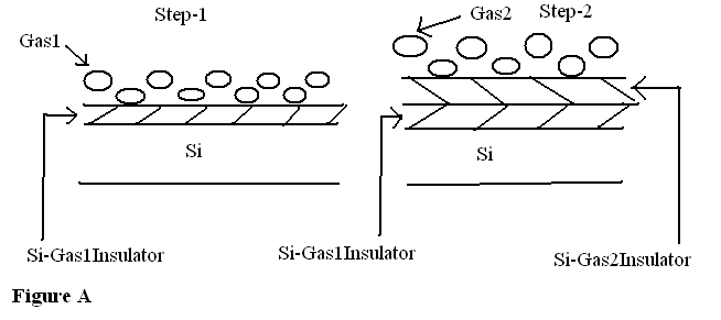
Figure VI.1. Methodology of Atomic Layer Deposition.
In Figure VI.1 the steps taken for Atomic Layer Deposition is illustrated. Gas1 reacts with bare Silicon surface to form a single atomic layer of insulator Si-Gas1. As soon as one layer is completed Gas1 stops reacting with Si because no bare Si is in contact with Gas1.
In step 2, Gas2 is chosen which is reactive with dielectric1 or Si-Gas1 insulator. Gas2 reacts with dielectric layer1 to form dielectric layer2 (Dielectric1-Gas2 insulator). As soon as dielectric layer2 covers the whole of dielectric1, reaction stops. Thus each reaction is terminated at the end of layer deposition. In this way we achieve layered gate insulator which is controllable down to the width of a single atom.
This produces much smoother dielectric hence the charge trapping is prevented . MOS produced is reproducible and stable in operation.
Appendix VII.
Fermi-level pinning and its prevention.
(academic.brooklyn.cuny.edu/physics/tung/Schottky/index.htm)
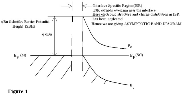
At Metal-ntype-Semiconductor interface we realize Schottky Barrier Diode. This exhibits a rectifying contact characteristic hence it has an in-built Schottky Barrier Height(SBH) as illustrated in Figure VII.1.

Figure VII.1. Asymptotic Energy Band Diagram of Metal-Semiconductor Interface and illustration of Schottky Barrier Potential Height.
It was found experimentally that SBH is insensitive to the Metal Work Function. This was defined as Fermi-Level pinning (FL pinning). It generally occurred at the mid-band gap of Semiconductor. This was always the case with polycrystalline MS interfaces and it was quite counterintuitive. In 1980s a few high quality, single crystal MS interfaces prepared and SBH measured. SBH was found to be sensitive to orientation/structure of of MS interface. By spatially-resolved SBH measurement technique notably by Ballistic Electron Emission Microscopy(BEEM) it was found that SBH are inhomogeneous at polycrystalline MS interfaces and structure dependent at single crystal MS interfaces.
At the turn of the century when dipole associated with chemical bonding at MS interfaces was modeled using established methods borrowed from Molecular Physics it was shown that FL pinning was a natural consequence of interfacial bonding.
If minimization of total energy is applied
By this theory FL pinning at polycrystalline MS interfaces and the pinning position at mid-band gap
comes automatically.
This model is being further refined.

Notification Switch
Would you like to follow the 'Solid state physics and devices-the harbinger of third wave of civilization' conversation and receive update notifications?