| << Chapter < Page | Chapter >> Page > |
Scanning tunneling microscopy (STM) is a powerful instrument that allows one to image the sample surface at the atomic level. As the first generation of scanning probe microscopy (SPM), STM paves the way for the study of nano-science and nano-materials. For the first time, researchers could obtain atom-resolution images of electrically conductive surfaces as well as their local electric structures. Because of this milestone invention, Gerd Binnig ( [link] ) and Heinrich Rohrer ( [link] ) won the Nobel Prize in Physics in 1986.


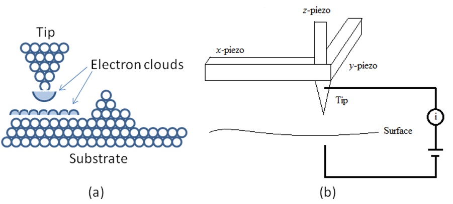
The key physical principle behind STM is the tunneling effect . In terms of their wave nature, the electrons in the surface atoms actually are not as tightly bonded to the nucleons as the electrons in the atoms of the bulk. More specifically, the electron density is not zero in the space outside the surface, though it will decrease exponentially as the distance between the electron and the surface increases ( [link] a). So, when a metal tip approaches to a conductive surface within a very short distance, normally just a few Å, their perspective electron clouds will starting to overlap, and generate tunneling current if a small voltage is applied between them, as shown in [link] b.

When we consider the separation between the tip and the surface as an ideal one-dimensional tunneling barrier, the tunneling probability, or the tunneling current I , will depend largely on s , the distance between the tip and surface, [link] , where m is the electron mass, e the electron charge, h the Plank constant, ϕ the averaged work function of the tip and the sample, and V the bias voltage.
A simple calculation will show us how strongly the tunneling current is affected by the distance ( s ). If s is increased by ∆s = 1 Å, [link] and [link] .
Usually (<ϕ>-e|V|/2) is about 5 eV, which k 0 about 1 Å -1 , then ∆I/I = 1 / 8 . That means, if s changes by 1 Å, the current will change by one order of the magnitude. That’s the reason why we can get atom-level image by measuring the tunneling current between the tip and the sample.
In a typical STM operation process, the tip is scanning across the surface of sample in x-y plain, the instrument records the x-y position of the tip, measures the tunneling current, and control the height of the tip via a feedback circuit. The movements of the tip in x, y and z directions are all controlled by piezo ceramics, which can be elongated or shortened according to the voltage applied on them.
Normally, there are two modes of operation for STM, constant height mode and constant current mode . In constant height mode, the tip stays at a constant height when it scans through the sample, and the tunneling current is measured at different ( x, y ) position ( [link] b). This mode can be applied when the surface of sample is very smooth. But, if the sample is rough, or has some large particles on the surface, the tip may contact with the sample and damage the surface. In this case, the constant current mode is applied. During this scanning process, the tunneling current, namely the distance between the tip and the sample, is settled to an unchanged target value. If the tunneling current is higher than that target value, that means the height of the sample surface is increasing, the distance between the tip and sample is decreasing. In this situation, the feedback control system will respond quickly and retract the tip. Conversely, if the tunneling current drops below the target value, the feedback control will have the tip closer to the surface. According to the output signal from feedback control, the surface of the sample can be imaged.

Notification Switch
Would you like to follow the 'Nanomaterials and nanotechnology' conversation and receive update notifications?