| << Chapter < Page | Chapter >> Page > |
Although, TEMs can only provide 2D analysis for a 3D specimen; magnifications of 300,000 times can be routinely obtained for many materials making it an ideal methodfor the study of nanomaterials. Besides from the TEM images, darker areas of the image show that the sample is thicker or denser in these areas, so we can observe the different components and structures of the specimen by the difference of color. For investigating multilayer-nanomaterials, a TEM is usually the first choice, because not only does it provide a high resolution image for nanomaterials but also it can distinguish each layer within a nanostructured material.
TEM was been used to analyze the depth-graded W/Si multilayer films. Multilayer films were grown on polished, 100 mm thick Si wafers by magnetron sputtering in argon gas. The individual tungsten and silicon layer thicknesses in periodic and depth-graded multilayers are adjusted by varying the computer-controlled rotational velocity of the substrate platen. The deposition times required to produce specific layer thicknesses were determined from detailed rate calibrations. Samples for TEM were prepared by focused ion beam milling at liquid N 2 temperature to prevent any beam heating which might result in re-crystallization and/or re-growth of any amorphous or fine grained polycrystalline layers in the film.
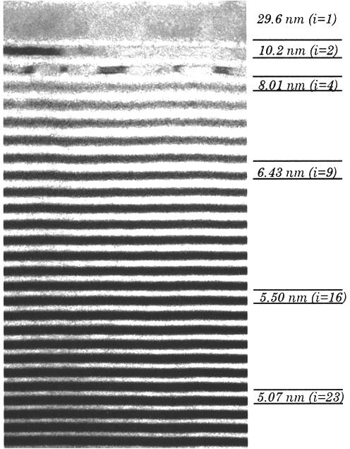
TEM measurements were made using a JEOL-4000 high-resolution transmission electron microscope operating at 400 keV; this instrument has a point-to-point resolution of 0.16 nm. Large area cross-sectional images of a depth-graded multilayer film obtained under medium magnification (~100 kX) were acquired at high resolution. A cross-sectional TEM image showed 150 layers W/Si film with the thickness of layers in the range of 3.33 ~ 29.6 nm ( [link] shows a part of layers). The dark layers are tungsten and the light layers are silicon and they are separated by the thin amorphous W–Si interlayers (gray bands). By the high resolution of the TEM and the nature characteristics of the material, each layer can be distinguished clearly with their different darkness.

Not all kinds of multilayer nanomaterials can be observed clearly under TEM. A materials consist of pc-Si:H multilayers were prepared by a photo-assisted chemical vapor deposition (photo-CVD) using a low-pressure mercury lamp as an UV light source to dissociate the gases. The pc-Si:H multilayer included low H 2 -diluted a-Si:H sublayers (SL’s) and highly H 2 -diluted a-Si:H sublayers (SH’s). Control of the CVD gas flow (H 2 |SiH 4 ) under continuous UV irradiation resulted in the deposition of multilayer films layer by layer.
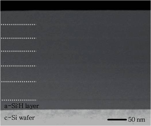
For a TEM measurement, a 20 nm thick undiluted a-Si:H film on a c-Si wafer before the deposition of multilayer to prevent from any epitaxial growth. [link] shows a cross-sectional TEM image of a six-cycled pc-Si:H multilayer specimen. The white dotted lines are used to emphasize the horizontal stripes, which have periodicity in the TEM image. As can be seen, there are no significant boundaries between SL and SH could be observed because all sublayers are prepared in H 2 gas. In order to get the more accurate thickness of each sublayer, other measurements might be necessary.


Notification Switch
Would you like to follow the 'Nanomaterials and nanotechnology' conversation and receive update notifications?