| << Chapter < Page | Chapter >> Page > |
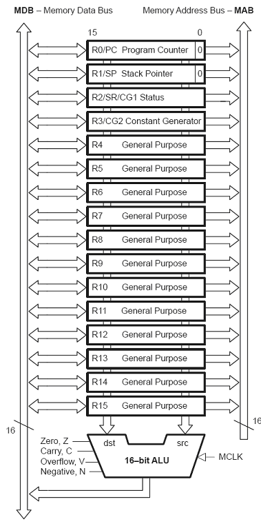
The RISC type architecture of the CPU is based on a short instruction set (27 instructions), interconnected by a 3-stage instruction pipeline for instruction decoding. The CPU has a 16-bit ALU, four dedicated registers and twelve working registers, which makes the MSP430 a high performance microcontroller suitable for low power applications. The addition of twelve working general purpose registers saves CPU cycles by allowing the storage of frequently used values and variables instead of using RAM.
The orthogonal instruction set allows the use of any addressing mode for any instruction, which makes programming clear and consistent, with few exceptions, increasing the compiler efficiency for high-level languages such as C.
Msp430 cpu block diagram.

The MSP430 CPU includes an arithmetic logic unit (ALU) that handles addition, subtraction, comparison and logical (AND, OR, XOR) operations. ALU operations can affect the overflow, zero, negative, and carry flags in the status register.
The CPU incorporates sixteen 16-bit registers:
- Four registers (R0, R1, R2 and R3) have dedicated functions;
- There are 12 working registers (R4 to R15) for general use.
The 16-bit Program Counter (PC/R0) points to the next instruction to be read from memory and executed by the CPU. The Program counter is implemented by the number of bytes used by the instruction (2, 4, or 6 bytes, always even). It is important to remember that the PC is aligned at even addresses, because the instructions are 16 bits, even though the individual memory addresses contain 8-bit values.
The Stack Pointer (SP/R1) is located in R1.
1 st : stack can be used by user to store data for later use (instructions: store by PUSH, retrieve by POP);
2 nd : stack can be used by user or by compiler for subroutine parameters (PUSH, POP in calling routine; addressed via offset calculation on stack pointer (SP) in called subroutine);
3 rd : used by subroutine calls to store the program counter value for return at subroutine's end (RET);
4 th : used by interrupt - system stores the actual PC value first, then the actual status register content (on top of stack) on return from interrupt (RETI) the system get the same status as just before the interrupt happened (as long as none has changed the value on TOS) and the same program counter value from stack.
The Status Register (SR/R2) stores the state and control bits. The system flags are changed automatically by the CPU depending on the result of an operation in a register. The reserved bits of the SR are used to support the constants generator. See the device-specific data sheets for more details.
SR
| 15 | 14 | 13 | 12 | 11 | 10 | 9 | 8 | 7 | 6 | 5 | 4 | 3 | 2 | 1 | 0 |
| Reserved for CG1 | V | SCG1 | SCG0 | OSCOFF | CPUOFF | GIE | N | Z | C |
| Bit | Description | |
| 8 | V | Overflow bit.V = 1 ⇒ Result of an arithmetic operation overflows the signed-variable range. |
| 7 | SCG1 | System clock generator 0.SCG1 = 1 ⇒ DCO generator is turned off – if not used for MCLK or SMCLK. |
| 6 | SCG0 | System clock generator 1.SCG0 = 1 ⇒ FLL+ loop control is turned off. |
| 5 | OSCOFF | Oscillator Off.OSCOFF = 1 ⇒ turns off LFXT1 when it is not used for MCLK or SMCLK. |
| 4 | CPUOFF | CPU off.CPUOFF = 1 ⇒ disable CPU core. |
| 3 | GIE | General interrupt enable.GIE = 1 ⇒ enables maskable interrupts. |
| 2 | N | Negative flag.N = 1 ⇒ result of a byte or word operation is negative. |
| 1 | Z | Zero flag.Z = 1 ⇒ result of a byte or word operation is 0. |
| 0 | C | Carry flag.C = 1 ⇒ result of a byte or word operation produced a carry. |
R2/R3: Constant Generator Registers (CG1/CG2)
Depending of the source-register addressing modes (As) value, six commonly used constants can be generated without a code word or code memory access to retrieve them.
This is a very powerful feature, which allows the implementation of emulated instructions, for example, instead of implementing a core instruction for an increment, the constant generator is used.
| Register | As | Constant | Remarks |
| R2 | 00 | - | Register mode |
| R2 | 01 | (0) | Absolute mode |
| R2 | 10 | 00004h | +4, bit processing |
| R2 | 11 | 00008h | +8, bit processing |
| R3 | 00 | 00000h | 0, word processing |
| R3 | 01 | 00001h | +1 |
| R3 | 10 | 00002h | +2, bit processing |
| R3 | 11 | 0FFFFh | -1, word processing |
These general-purpose registers are used to store data values, address pointers, or index values and can be accessed with byte or word instructions.
Request the MSP430 Teaching ROM Materials here (External Link)

Notification Switch
Would you like to follow the 'Teaching and classroom laboratories based on the “ez430” and "experimenter's board" msp430 microcontroller platforms and code composer essentials' conversation and receive update notifications?