| << Chapter < Page | Chapter >> Page > |
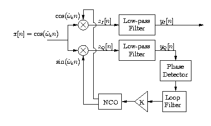
After gaining a theoretical understanding of the carrier recovery sub-system of a digital receiver, you will simulate the sub-system in MATLAB and implement it on the DSP. Thesub-system described is specifically tailored to a non-modulated carrier. A complete implementation will requiremodifications to the design presented.
The phase-locked loop ( PLL ) is a critical component in coherent communications receivers thatis responsible for locking on to the carrier of a received modulated signal. Ideally, the transmitted carrier frequencyis known exactly and we need only to know its phase to demodulate correctly. However, due to imperfections at thetransmitter, the actual carrier frequency may be slightly different from the expected frequency. For example, in theQPSK transmitter of Digital Transmitter: Introduction to Quadrature Phase-ShiftKeying , if the digital carrier frequency is and the D/A is operating at 44.1 kHz, then the expected analog carrier frequency is . If there is a slight change to the D/A sample rate (say ), then there will be a corresponding change in the actual analog carrier frequency( ).
This difference between the expected and actual carrier frequencies can be modeled as a time-varying phase. Providedthat the frequency mismatch is small relative to the carrier frequency, the feedback control of an appropriately calibratedPLL can track this time-varying phase, thereby locking on to both the correct frequency and the correct phase.

In a complete coherent receiver implementation, carrier recovery is required since the receiver typically does notknow the exact phase and frequency of the transmitted carrier. In an analog system this recovery is oftenimplemented with a voltage-controlled oscillator ( VCO ) that allows for precise adjustment of the carrier frequency based on the output of aphase-detecting circuit.
In our digital application, this adjustment is performed with a numerically-controlled oscillator ( NCO ) (see [link] ). A simple scheme for implementing an NCO is based on the followingre-expression of the carrier sinusoid:

Notification Switch
Would you like to follow the 'Dsp laboratory with ti tms320c54x' conversation and receive update notifications?