| << Chapter < Page | Chapter >> Page > |
| Element | Bayer process (ppm) | After acid/base leaching (ppm) | 500 zone passes (ppm) |
| aluminum | 100-1,000 | 7 | <1 |
| calcium | 10-100 | not detected | not detected |
| copper | 100-1,000 | 2 | <1 |
| iron | 100-1,000 | 7 | <1 |
| lead | <2000 | 30 | not detected |
| magnesium | 10-100 | 1 | not detected |
| mercury | 10-100 | not detected | not detected |
| nickel | 10-100 | not detected | not detected |
| silicon | 10-100 | ≈ 1 | not detected |
| tin | 10-100 | ≈ 1 | not detected |
| titanium | 10-100 | 1 | <1 |
| zinc | 30,000 | ≈ 1 | not detected |

Elemental arsenic (L. arsenicum, yellow orpiment) exists in two forms: yellow (cubic, As 4 ) and gray or metallic (rhombohedral). At a natural abundance of 1.8 ppm arsenic is relatively rare, however, this is offset by its presence in a number of common minerals and the relative ease of isolation. Arsenic containing minerals are grouped into three main classes: the sulfides realgar (As 4 S 4 ) and orpiment (As 2 S 3 ), the oxide arsenolite (As 2 O 3 ), and the arsenides and sulfaresenides of the iron, cobalt, and nickel. Minerals in this latter class include: loellinginite (FeAs 2 ), safforlite (CoAs), niccolite (NiAs), rammelsbergite (NiAs 2 ), ansenopyrite or mispickel (FeAsS), cobaltite (CoAsS), enargite (Cu 3 AsS 4 ), gerdsorfite (NiAsS), and the quarturnary sulfide glaucodot [(Co,Fe)AsS]. [link] shows the typical impurities in arsenopyrite.
| Element | Concentration (ppm) | Element | Concentration (ppm) |
| silver | 90 | nickel | <3,000 |
| gold | 8 | lead | 50 |
| cobalt | 30,000 | platinum | 0.4 |
| copper | 200 | rhenium | 50 |
| germanium | 30 | selenium | 50 |
| manganese | 3,000 | vanadium | 300 |
| molybdenum | 60 | zinc | 400 |
Arsenic is obtained commercially by smelting either FeAs 2 or FeAsS at 650-700 °C in the absence of air and condensing the sublimed element (T sub = 613 °C), [link] .
The arsenic thus obtained is combined with lead and then sublimed (T sub = 614 °C) which binds any sulfur impurities more strongly than arsenic. Any residual arsenic that remains trapped in the iron sulfide is separated by forming the oxide (As 2 O 3 ) by roasting the sulfide in air. The oxide is sublimed into the flue system during roasting from where it is collected and reduced with charcoal at 700-800 °C to give elemental arsenic. Semiconductor grade arsenic (>99.9999%) is formed by zone refining.
Gallium arsenide can be prepared by the direct reaction of the elements, [link] . However, while conceptually simple the synthesis of GaAs is complicated by the different vapor pressures of the reagents and the highly exothermic nature of the reaction. Furthermore, since the synthesis of GaAs at atmospheric pressure is accompanied by its simultaneous decomposes due to the loss by sublimation, of arsenic, the synthesis must be carried out under an overpressure of arsenic in order to maintain a stoichiometric composition of the synthesized GaAs.
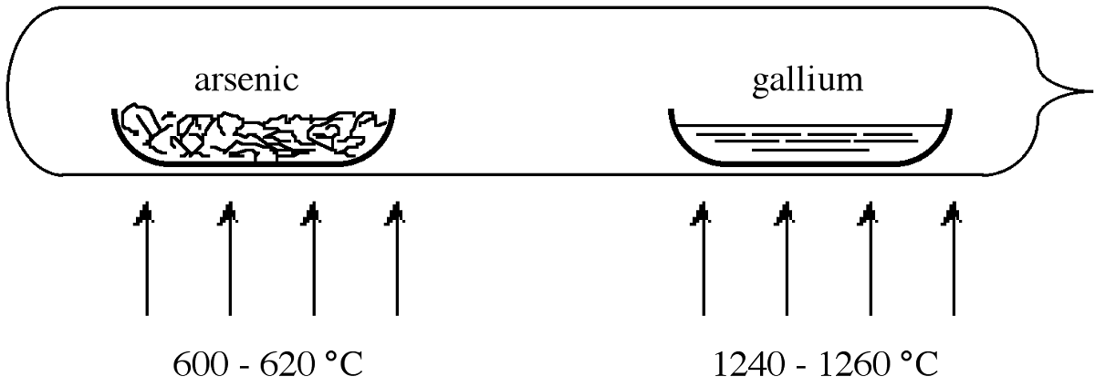
In order to overcome the problems associated with arsenic loss, the reaction is usually carried out in a sealed reaction tube. However, if a stoichiometric quantity of arsenic is used in the reaction a constant temperature of 1238 °C must be employed in order to maintain the desired arsenic overpressure of 1 atm. Practically, it is easier to use a large excess of arsenic heated to a lower temperature. In this situation the pressure in the tube is approximately equal to the equilibrium vapor pressure of the volatile component (arsenic) at the lower temperature. Thus, an over pressure of 1 atm arsenic may be maintained if within a sealed tube elemental arsenic is heated to 600-620 °C while the GaAs is maintained at 1240-1250 °C.
[link] shows the sealed tube configuration that is typically used for the synthesis of GaAs. The tube is heated within a two-zone furnace. The boats holding the reactants are usually made of quartz, however, graphite is also used since the latter has a closer thermal expansion match to the GaAs product. If higher purity is required then pyrolytic boron nitride (PBN) is used. One of the boats is loaded with pure gallium the other with arsenic. A plug of quartz wool may be placed between the boats to act as a diffuser. The tube is then evacuated and sealed. Once brought to the correct reaction temperatures ( [link] ), the arsenic vapor is transported to the gallium, and they react to form GaAs in a controlled manner. [link] gives the typical impurity concentrations found in polycrystalline GaAs.

| Element | Concentration (ppm) | Element | Concentration (ppm) |
| boron | 0.1 | silicon | 0.02 |
| carbon | 0.7 | phosphorus | 0.1 |
| nitrogen | 0.1 | sulfur | 0.01 |
| oxygen | 0.5 | chlorine | 0.08 |
| fluorine | 0.2 | nickel | 0.04 |
| magnesium | 0.02 | copper | 0.01 |
| aluminum | 0.02 | zinc | 0.05 |
Polycrystalline GaAs, formed in from the direct reaction of the elements is often used as the starting material for single crystal growth

Notification Switch
Would you like to follow the 'Chemistry of electronic materials' conversation and receive update notifications?