| << Chapter < Page | Chapter >> Page > |
When considering the synthesis of Group 13-15 compounds for electronic applications, the very nature of semiconductor behavior demands the use of high purity single crystal materials. The polycrystalline materials synthesized above are, therefore, of little use for 13-15 semiconductors but may, however, serve as the starting material for melt grown single crystals. For GaAs, undoubtedly the most important 13-15 (III - V) semiconductor, melt grown single crystals are achieved by one of two techniques: the Bridgman technique, and the Czochralski technique.
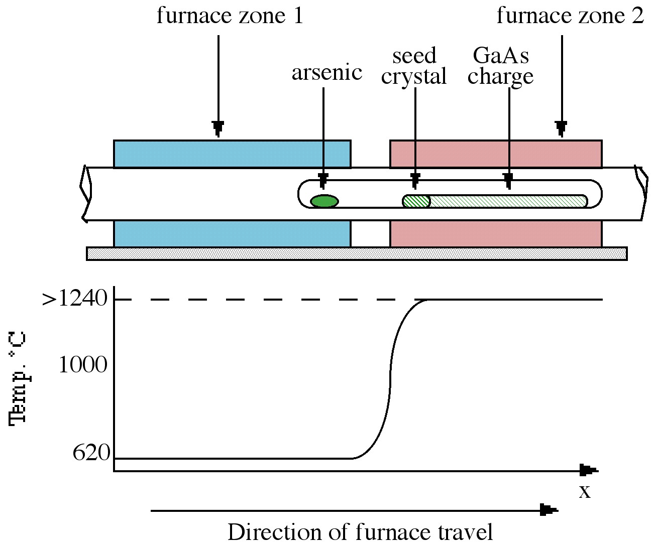
The Bridgman technique requires a two-zone furnace, of the type shown in [link] . The left hand zone is maintained at a temperature of ca . 610 °C, allowing sufficient overpressure of arsenic within the sealed system to prevent arsenic loss from the gallium arsenide. The right hand side of the furnace contains the polycrystalline GaAs raw material held at a temperature just above its melting point ( ca . 1240 °C). As the furnace moves from left to right, the melt cools and solidifies. If a seed crystal is placed at the left hand side of the melt (at a point where the temperature gradient is such that only the end melts), a specific orientation of single crystal may be propagated at the liquid-solid interface eventually to produce a single crystal.

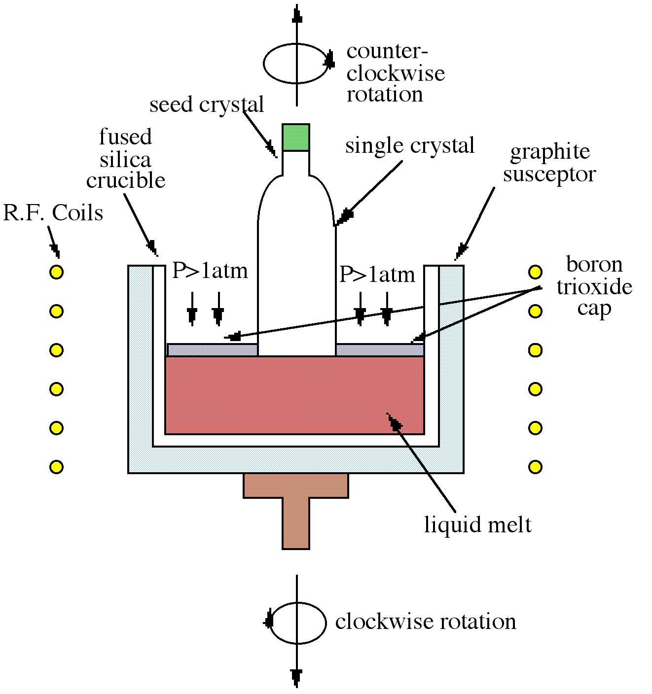
The Czochralski technique, which is the most commonly used technique in industry, is shown in [link] . The process relies on the controlled withdrawal of a seed crystal from a liquid melt. As the seed is lowered into the melt, partial melting of the tip occurs creating the liquid solid interface required for crystal growth. As the seed is withdrawn, solidification occurs and the seed orientation is propagated into the grown material. The variable parameters of rate of withdrawal and rotation rate can control crystal diameter and purity. As shown in [link] the GaAs melt is capped by boron trioxide (B 2 O 3 ). The capping layer, which is inert to GaAs, prevents arsenic loss when the pressure on the surface is above atmospheric pressure. The growth of GaAs by this technique is thus termed liquid encapsulated Czochralski (LEC) growth.

While the Bridgman technique is largely favored for GaAs growth, larger diameter wafers can be obtained by the Czochralski method. Both of these melt techniques produce materials heavily contaminated by the crucible, making them suitable almost exclusively as substrate material. Another disadvantage of these techniques is the production of defects in the material caused by the melt process.

Notification Switch
Would you like to follow the 'Chemistry of electronic materials' conversation and receive update notifications?